Apparatus and method for measuring spectral reflectance and apparatus for measuring film thickness

a technology of spectral reflectance and measurement apparatus, which is applied in the direction of optical radiation measurement, interferometric spectrometry, instruments, etc., can solve the problems of measurement accuracy degradation and inability to obtain a reflectance on the basis of an image with accuracy, and achieve high accuracy

a technology of spectral reflectance and measurement apparatus, which is applied in the direction of optical radiation measurement, interferometric spectrometry, instruments, etc., can solve the problems of measurement accuracy degradation and inability to obtain a reflectance on the basis of an image with accuracy, and achieve high accuracy

US20050206907A1Inactive Publication Date: 2005-09-22DAINIPPON SCREEN MTG CO LTD

Image

  • Apparatus and method for measuring spectral reflectance and apparatus for measuring film thickness
  • Apparatus and method for measuring spectral reflectance and apparatus for measuring film thickness
  • Apparatus and method for measuring spectral reflectance and apparatus for measuring film thickness

Examples


Embodiment Construction

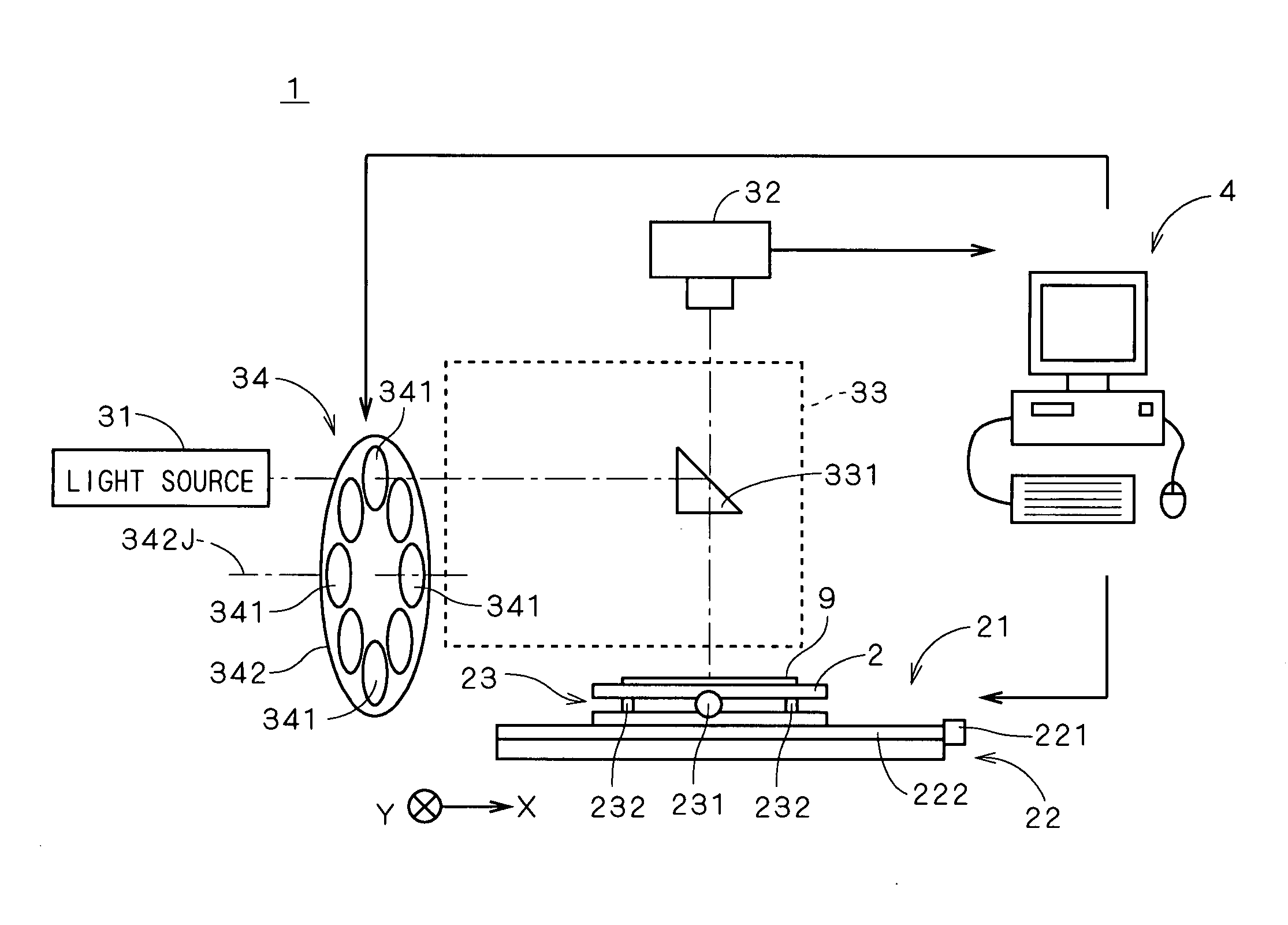
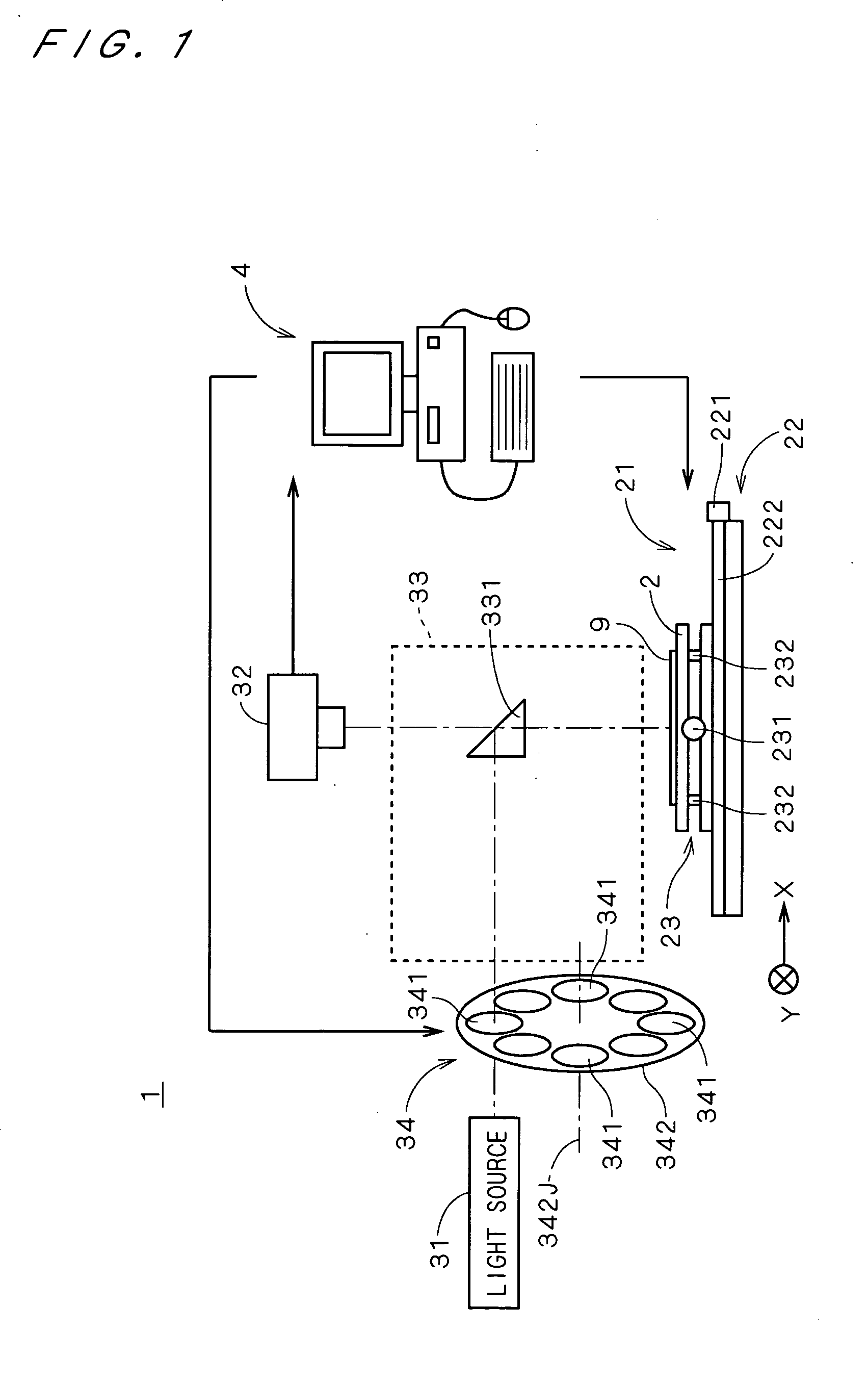
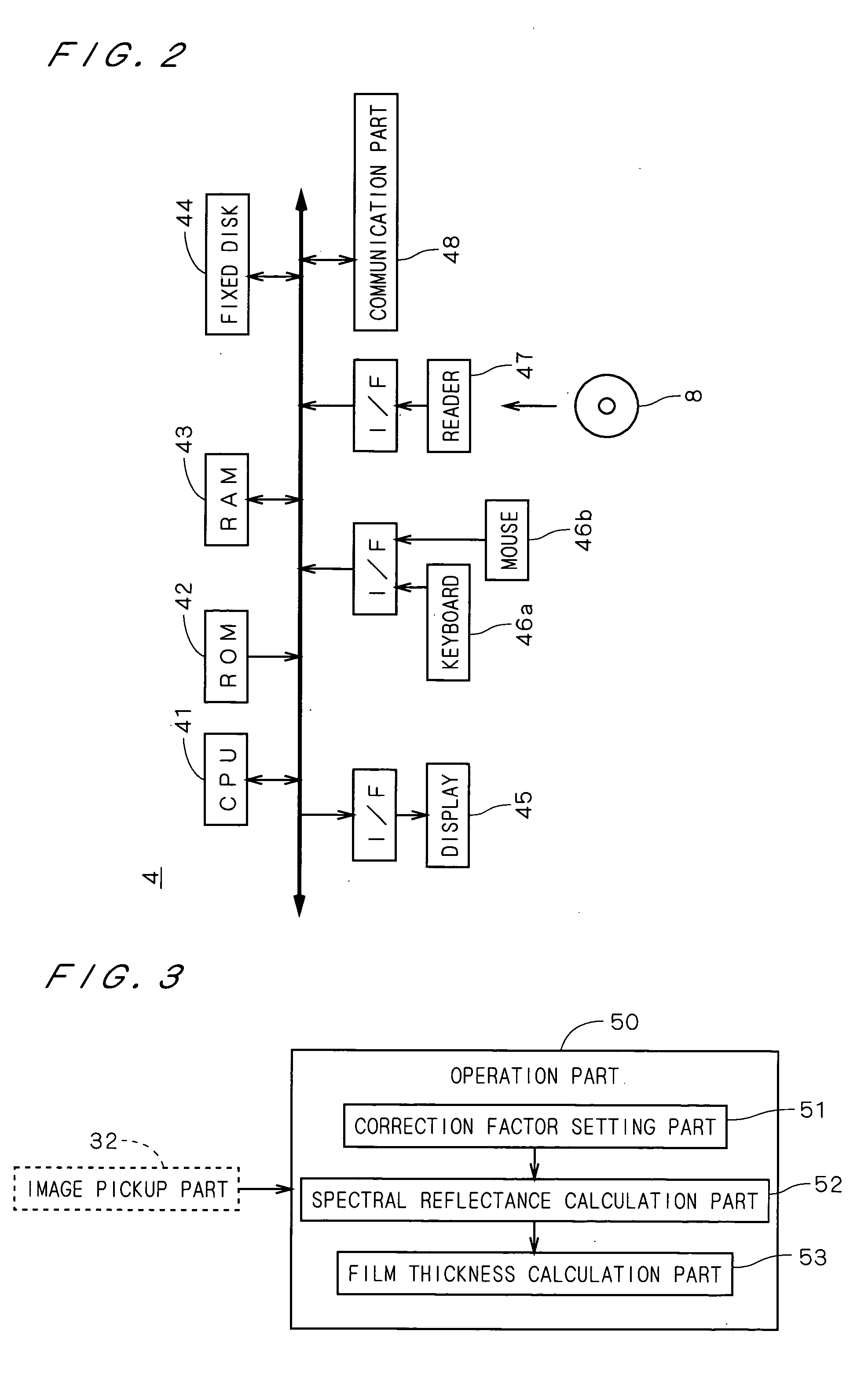
[0029]FIG. 1 is a view showing a construction of a film thickness measurement apparatus 1 in accordance with one preferred embodiment of the present invention. The film thickness measurement apparatus 1 comprises a stage 2 for holding a substrate 9 (e.g., a semiconductor substrate formed of Si (silicon)) with a thin film which is formed on its surface, a stage moving mechanism 21 for moving the stage 2 in X and Y directions of FIG. 1, a light source 31 for emitting light of multiple wavelengths (e.g., white light), an image pickup part 32 for picking up an image of the substrate 9, an optical system 33 for guiding light from the light source 31 onto the substrate 9 and guiding light reflected on the substrate 9 to the image pickup part 32 and a filter unit 34 having a plurality of filters 341 for transmitting lights of a plurality of different wavelengths (exactly, a plurality of lights included in a plurality of different wavelength bands). Though only a prism 331 is shown in FIG. ...


PUM


Abstract

A film thickness measurement apparatus has an image pickup part (32) for acquiring a plurality of single-band images corresponding to a plurality of wavelengths, and the image pickup part (32) acquires a plurality of reference single-band images representing a pattern on a reference substrate. A correction factor setting part (51) performs setting of a plurality of correction factors in accordance with distances from a specified pixel by using a plurality of reference single-band images. Subsequently, the image pickup part (32) acquires a plurality of measurement single-band images representing a pattern on an objective substrate and corrects a value of the specified pixel for each of a plurality of measurement single-band images by using the value of the specified pixel and values of pixels surrounding the specified pixel and the correction factors. A spectral reflectance calculation part (52) thereby calculates a reflectance at a measurement point on the objective substrate which corresponds to the specified pixel on the basis of the corrected value of the specified pixel with high accuracy.

Description

BACKGROUND OF THE INVENTION [0001] 1. Field of the Invention [0002] The present invention relates to a technique for measuring spectral reflectance of a measurement object and a technique for measuring a thickness of a film (or thicknesses of films) formed on a measurement object. [0003] 2. Description of the Background Art [0004] In order to ensure consistent quality of semiconductor products, it is usual to measure thicknesses of films (e.g., layered thin films) formed on a semiconductor substrate (hereinafter, referred to as “substrate”) in an inspection step of a semiconductor manufacturing process. For measurement of film thicknesses, a film thickness measurement apparatus has been conventionally used, adopting a light interferometric method where film thicknesses are calculated on the basis of spectral reflectance obtained by emitting white light to a substrate and performing spectrometric analysis of the light reflected on the substrate. [0005] Japanese Patent Application Lai...

Claims


Application Information

Patent Timeline
22 Sep 2005
Publication
US20050206907A1
IPC
G01B9/02; G01B11/06; G01N21/27
CPC
G01B11/0625
Inventors
FUJIMOTO, HIROKI; KONDO, NORIYUKI