Memory module system with efficient control of on-die termination

a memory module and efficient control technology, applied in the field of memory module systems, can solve the problems of signal reflection from impedance mismatch at an interface point becoming more critical, degraded impedance mismatch at an interface point, etc., and achieve the effect of reducing power consumption

Active Publication Date: 2005-09-29
SAMSUNG ELECTRONICS CO LTD
View PDF2 Cites 79 Cited by
  • Summary
  • Abstract
  • Description
  • Claims
  • Application Information

AI Technical Summary

Benefits of technology

[0029] In this manner, just one pin from the memory controller is used for sending command signals indicating one of the memory devices that is activated. The activated memory device then includes components that are turned on for generating the ODT control signal for controlling ODT circuits of inactivated memory devices. The components for generating an ODT control signal within the inactivated memory devices are turned off for minimized power consumption.

Problems solved by technology

However with such decreased swing width, influence of external noise increases such that signal reflection from impedance mismatch at an interface point becomes more critical.
Such an impedance mismatch degrades high-speed data transmission as output data from an output node of a semiconductor device is distorted.
Another semiconductor device receives the distorted output signal with possible setup / hold fail or misjudgment of input level.
Although the point-to-point connection structure provides optimum signal fidelity, a signal line is allocated to each connection such that the point-to-point connection structure may not be amenable for high-bandwidth data transmission.
However, as overall timing budget is decreasing for higher-speed memory systems, variance of signal fidelity among the ODT control methods becomes important.

Method used


Image

  • Memory module system with efficient control of on-die termination
  • Memory module system with efficient control of on-die termination
  • Memory module system with efficient control of on-die termination

Examples


Embodiment Construction

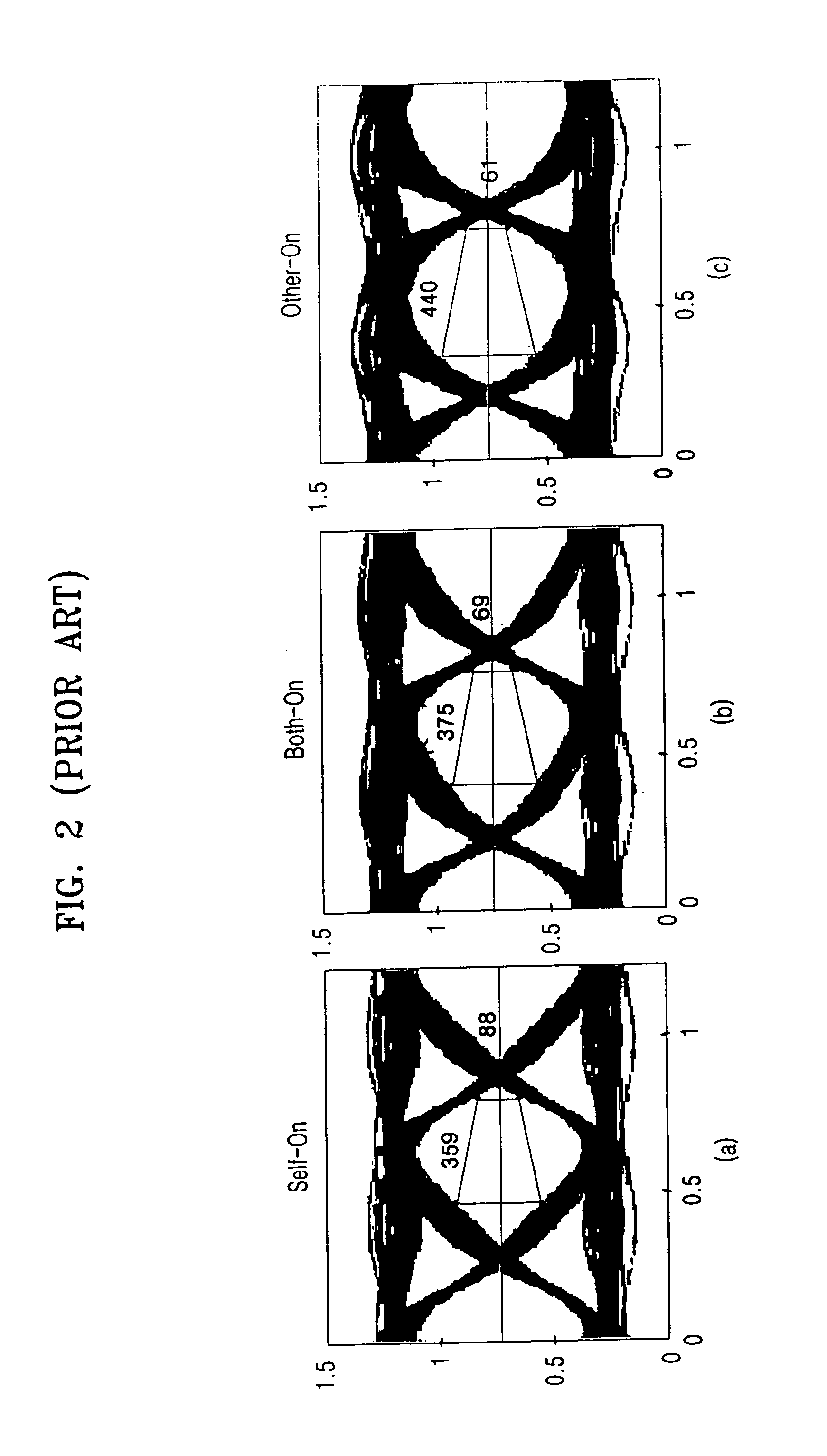
[0044] As shown in FIG. 2, the other-on control method results in the best signal fidelity characteristic in a dual rank memory system. However, with the other-on control method, an additional burden of a separate external resource may be needed for controlling the ODT (on-die termination) of an inactivated memory device. On the other hand for the self-on ODT control method, an internal element within a memory device translates a command for determining whether to activate the ODT within the memory device.

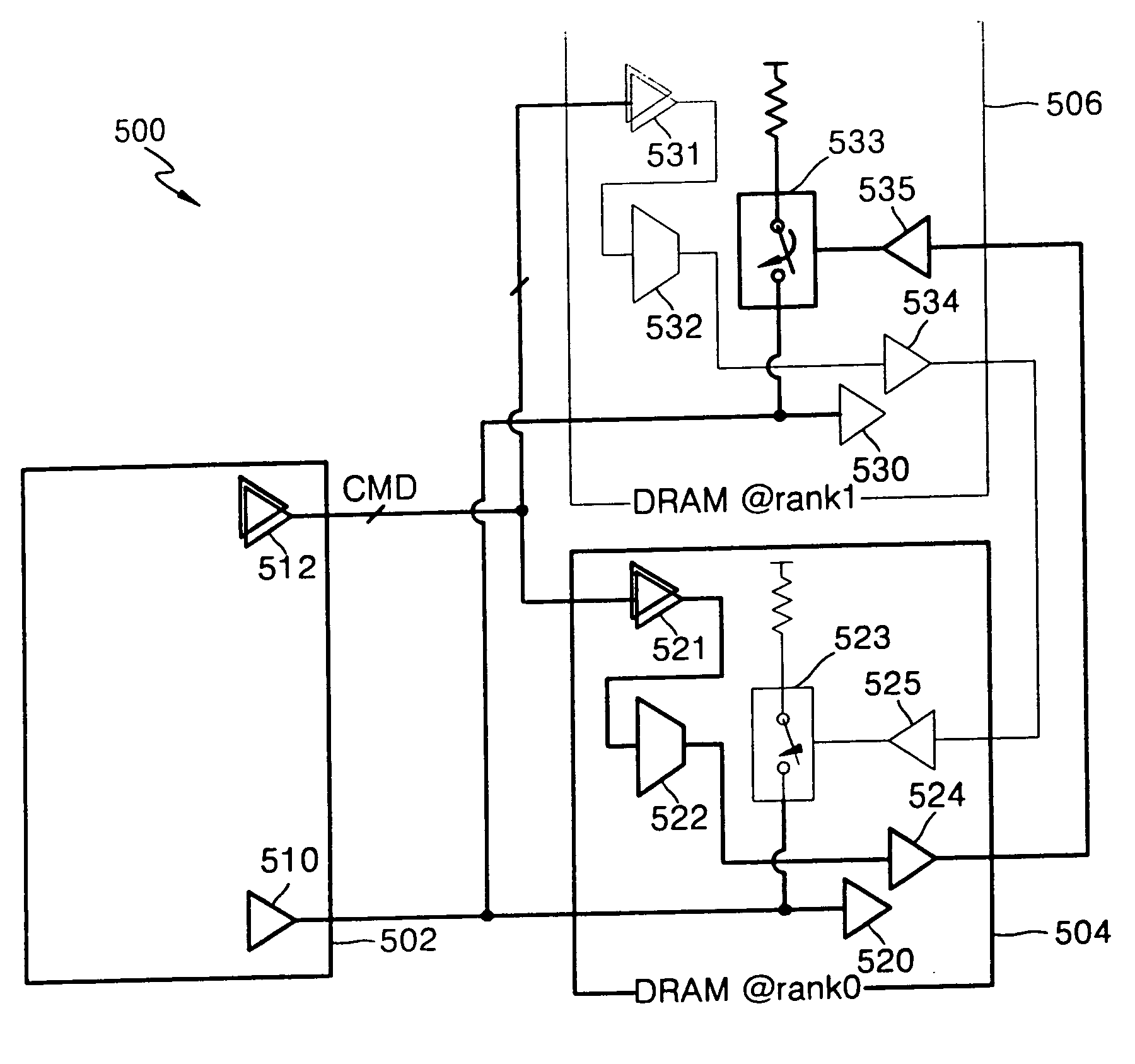
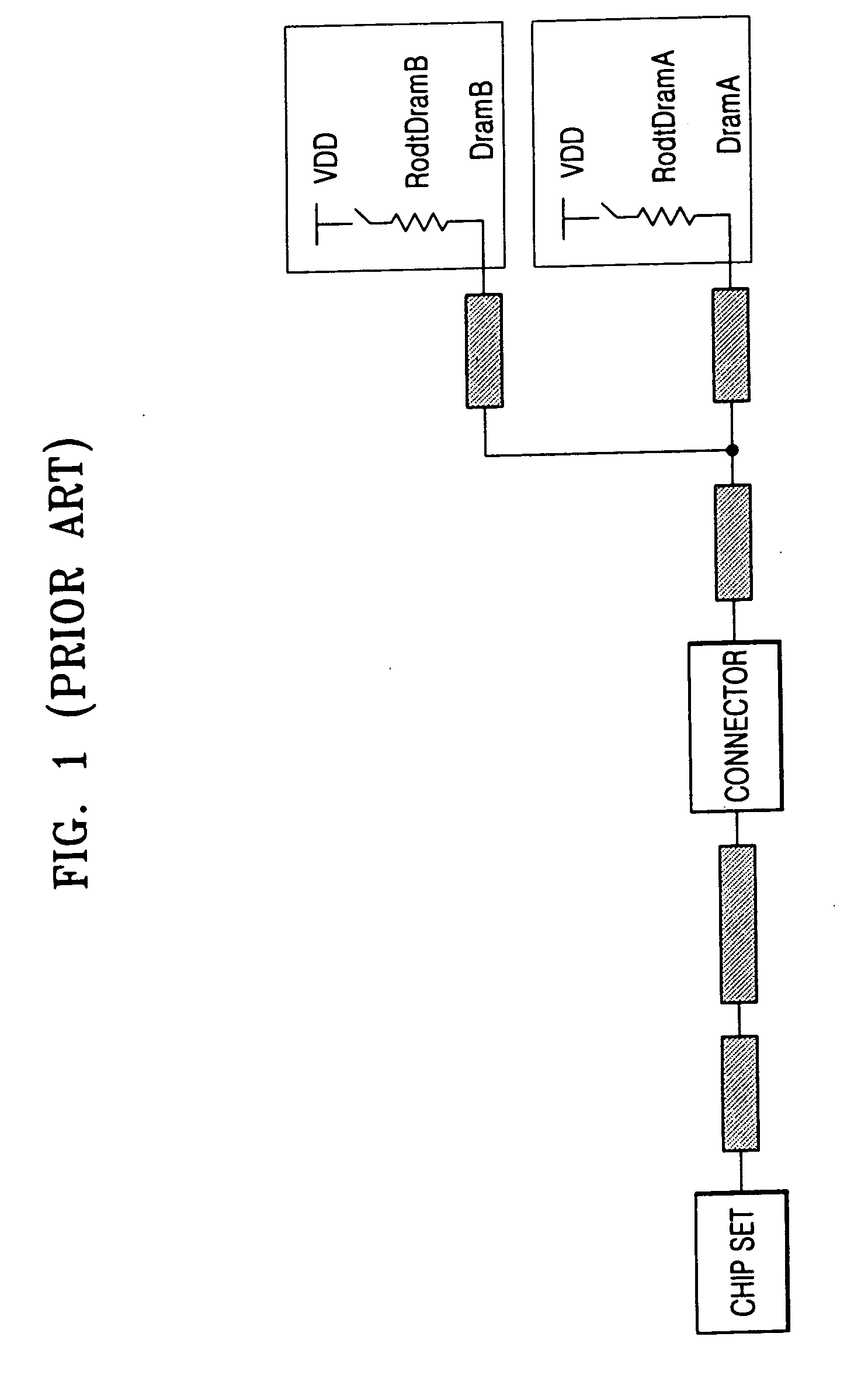
[0045]FIG. 3 is a circuit diagram of a dual rank memory system 300 having a separate resource for conventional ODT control. Referring to FIG. 3, the dual rank memory system 300 includes a memory controller 302, a first memory device 304, and a second memory device 306. The memory controller 302 selects one of the first and second memory devices 304 and 306 to be activated for storing / reading data.

[0046] The first memory device 304 is for a first rank “rank0”, and the second memor...


PUM


Abstract

For ODT (on-die termination) control within a memory module system, just one pin from the memory controller is used for sending command signals indicating an activated one of the memory devices. The activated memory device includes components that are turned on for generating the ODT control signal for controlling an ODT circuit of inactivated memory device(s). The components for generating an ODT control signal within the inactivated memory devices are turned off for minimized power consumption.

Description

BACKGROUND OF THE INVENTION [0001] This application claims priority to Korean Patent Application No. 2004-0020764, filed on Mar. 26, 2004, in the Korean Intellectual Property Office, the disclosure of which is incorporated herein in its entirety by reference. [0002] 1. Field of the Invention [0003] The present invention relates generally to memory module systems, and more particularly to a memory module system having an activated memory device controlling on-die termination of at least one inactivated memory device for efficient control.[0004] 2. Description of the Related Art [0005] Semiconductor devices include receiving circuits for receiving signals via input pads and include output circuits for outputting signals via output pads. Due to high operating speed, the swing width of signals exchanged between semiconductor devices is decreased to minimize delay time of signal transmission. [0006] However with such decreased swing width, influence of external noise increases such that ...

Claims


Application Information

Patent Timeline
Patent Type & Authority Applications(United States)
IPC IPC(8): G06F12/00G11C5/00G11C7/10G11C11/401H03K19/003H04L25/02
CPCG11C5/04H04L25/0278G11C7/1084G11C7/1078G11C7/1048G11C7/1051
Inventor SO, BYUNG-SECHO, JEONG-HYEONLEE, JAE-JUN
Owner SAMSUNG ELECTRONICS CO LTD
Why Eureka
Try Eureka