Bumping process, bump structure, packaging process and package structure

Inactive Publication Date: 2005-09-29
ADVANCED SEMICON ENG INC
View PDF14 Cites 21 Cited by
  • Summary
  • Abstract
  • Description
  • Claims
  • Application Information

AI Technical Summary

Benefits of technology

[0012] The present invention is directed to a bumping process, a bump structure, a packaging process and a package structure for in

Problems solved by technology

When the bumps are subjected to a shear stress that exceed its permissible limit, the bumps might crack leading to an open circuit in the electrical connection between the chip and the package substrate.
Furthermore, because the sidewalls of the openings in the photoresist layer for forming the bumps are almost perpendicular to the surface of the wafer, the amount of solder material inside

Method used


Image

  • Bumping process, bump structure, packaging process and package structure
  • Bumping process, bump structure, packaging process and package structure
  • Bumping process, bump structure, packaging process and package structure

Examples


Example

[0034] Reference will now be made in detail to the present preferred embodiments of the invention, examples of which are illustrated in the accompanying drawings. Wherever possible, the same reference numbers are used in the drawings and the description to refer to the same or like parts.

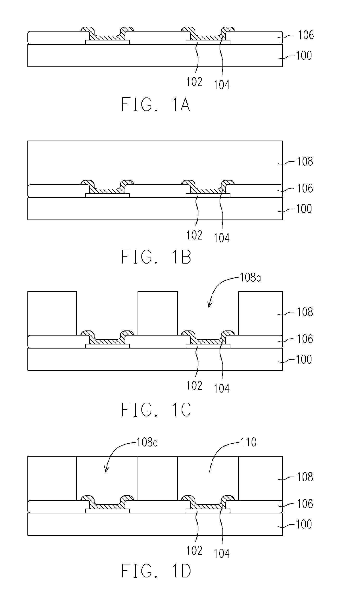
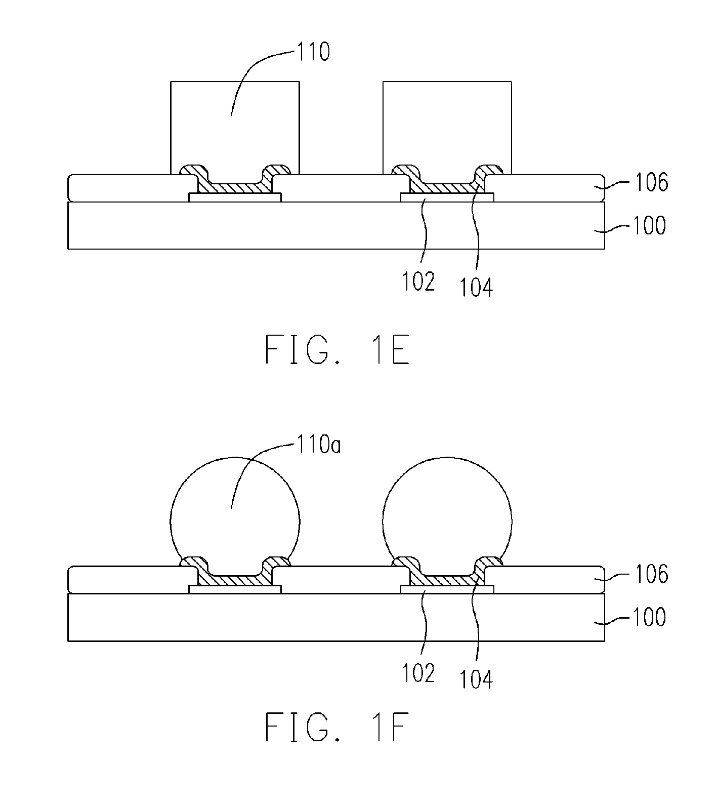
[0035]FIGS. 3A through 3F are schematic cross-sectional views showing the steps of fabricating a bump structure according to one embodiment of the present invention. First, as shown in FIG. 3A, a wafer 310 is provided. The wafer 310 has a plurality of bonding pads 314 and a passivation layer 316, wherein the passivation layer 316 protects the wafer 310 and exposes the bonding pads 314. Thereafter, a metallic layer 318 is formed over the wafer 318. The metallic layer 318 covers the bonding pads 314 and the passivation layer 316, for example.

[0036] The metallic layer 318 is formed in a sputtering or evaporation process, for example. The metallic layer 318 is a three-layer stacked structure comprisin...


PUM


Abstract

A bumping process, a bump structure, a packaging process and a package structure are described. The bump structure comprises a first solder portion, a second solder portion and a conductive layer. The second solder portion is disposed on the first solder portion and the conductive layer is disposed between the first solder portion and the second solder portion. The bumping process produces a bump structure having a greater height. The bumping process can also be applied in a package process to form a package structure having a highly reliable connection between a chip and a packaging substrate.

Description

CROSS-REFERENCE TO RELATED APPLICATION [0001] This application claims the priority benefit of Taiwan application serial no. 93108238, filed on Mar. 26, 2004. BACKGROUND OF THE INVENTION [0002] 1. Field of the Invention [0003] The present invention relates to a bumping process, a bump structure, a packaging process and a package structure. More particularly, the present invention relates to a bumping process, a bump structure, a packaging process and a package structure capable of increasing bump height so that a highly reliable connection between a chip and a packaging substrate is formed. [0004] 2. Description of Related Art [0005] Since communication has become increasingly important in the modern world, the market for multi-media systems continues to expand. To meet the demands of multi- media users, many types of integrated circuit packages have already incorporated digital, networking, local area communication and customization functions. In other words, the processing speed, f...

Claims


Application Information

Patent Timeline
IPC IPC(8): H01L21/44H01L21/56H01L21/60H01L23/485H05K3/34
CPCH01L21/563H01L24/13H01L2224/1147H01L2224/1308H01L2224/13111H01L2224/13116H01L2224/13147H01L2224/13155H01L2224/73203H01L2924/01013H01L2924/01022H01L2924/01029H01L2924/01047H01L2924/01082H01L2924/14H05K3/3436H05K3/3473H05K2201/0379H05K2201/1025H05K2203/043H01L24/11H01L2924/00013H01L2924/01006H01L2924/01023H01L2924/014H01L2924/01033H01L2924/00014H01L2924/0105H01L2224/13099H01L2924/351H01L2224/05022H01L2224/05001H01L2224/05572H01L2224/05624H01L2224/05647H01L2224/05666H01L24/05Y02P70/50H01L2224/73204H01L2924/00H01L2224/05099
Inventor HUNG, CHING-FU
Owner ADVANCED SEMICON ENG INC
Why Eureka
Try Eureka