

Reduction of channel hot carrier effects in transistor devices
a transistor and hot carrier technology, applied in the field of semiconductor devices, can solve the problems of gate dielectrics to store charge, channel hot carrier effects, field effect transistors, etc., and achieve the effect of reducing channel hot carrier effects and minimizing channel hot carriers
- Summary
- Abstract
- Description
- Claims
- Application Information
AI Technical Summary
Benefits of technology
Problems solved by technology
Method used
Image

Examples
Embodiment Construction
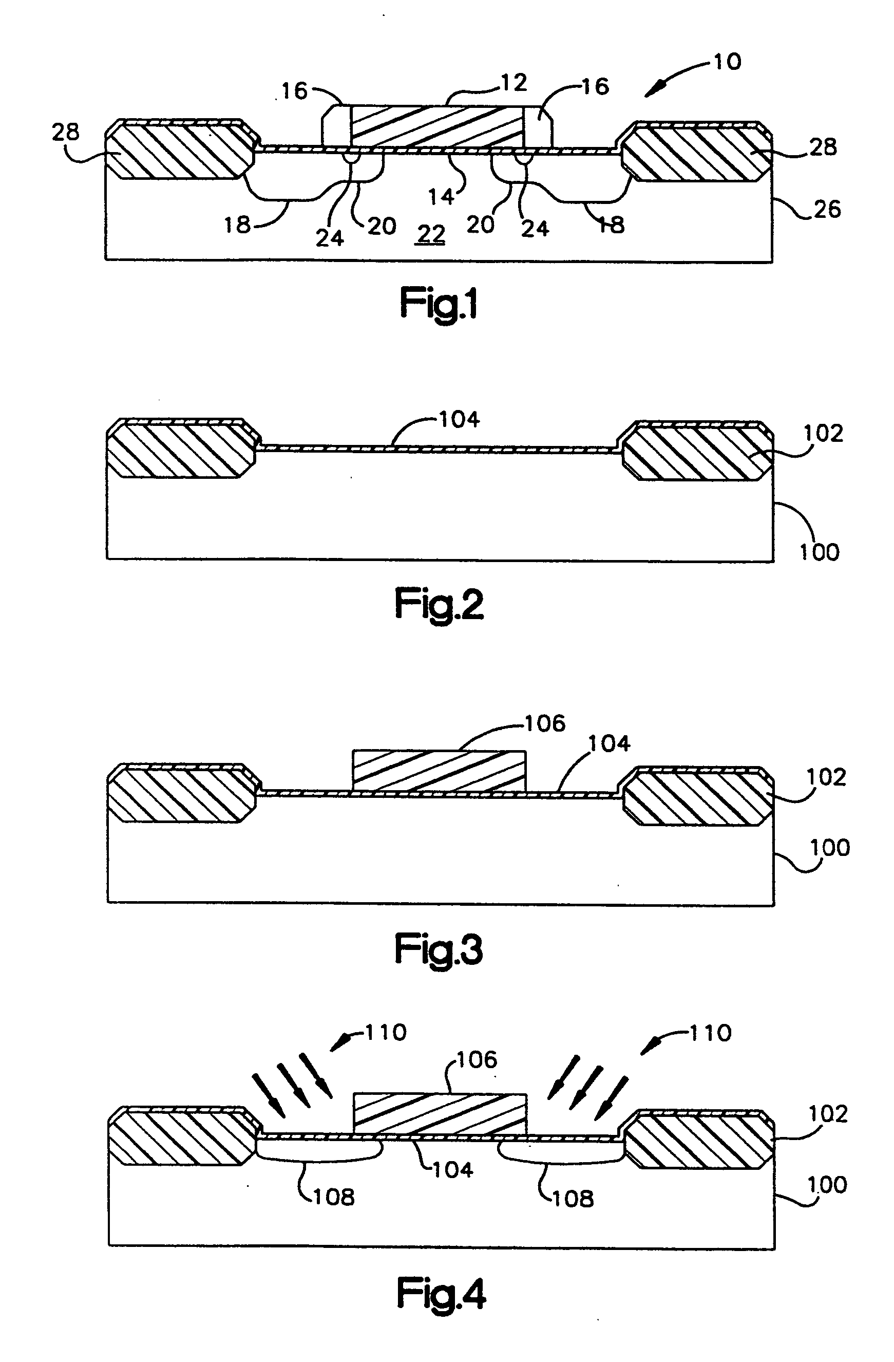
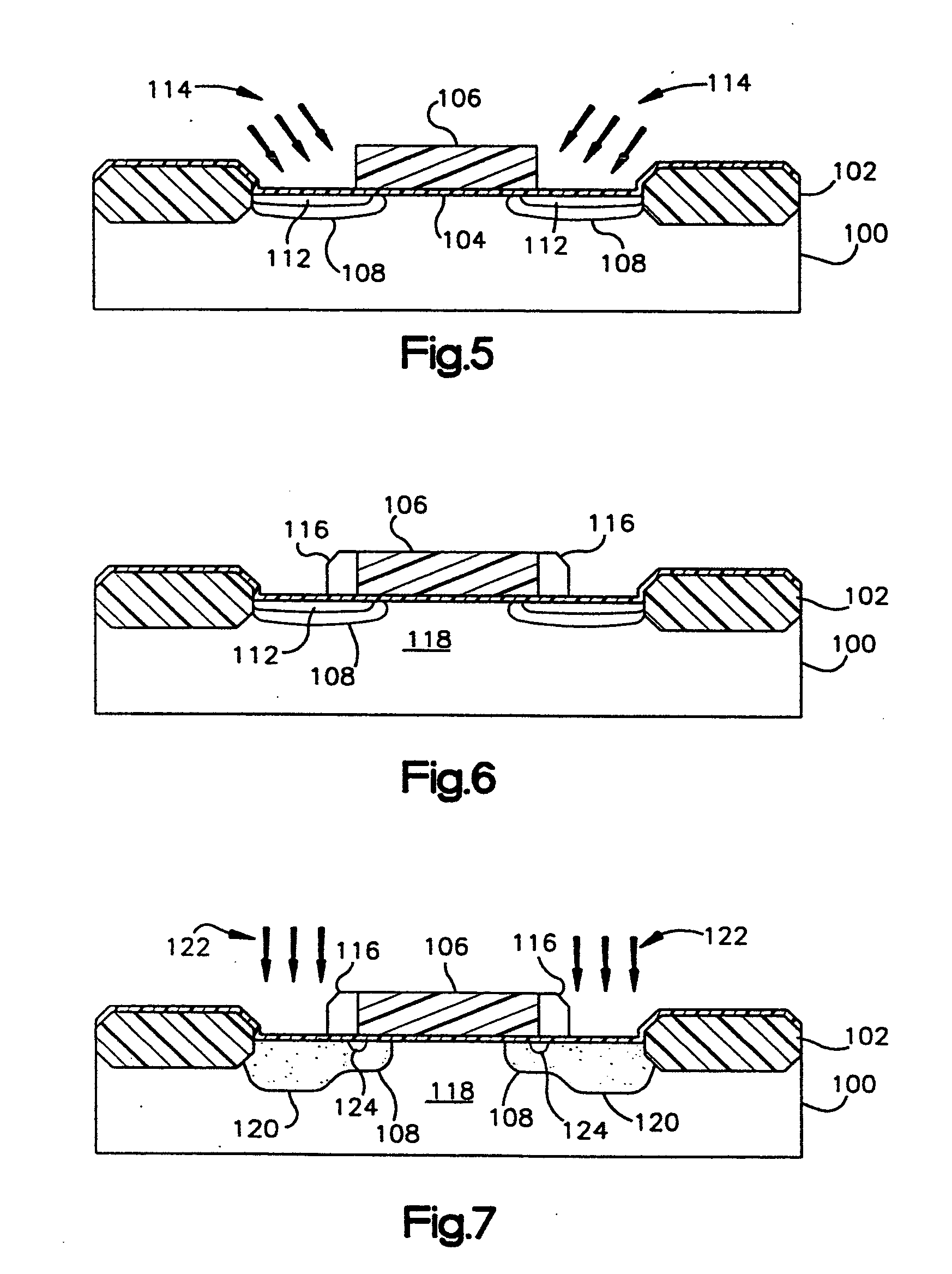
[0019] The present invention relates generally to a metal oxide semiconductor field effect transistor (MOSFET) that mitigates channel hot carriers or hot electrons. This is achieved by employing a shallow floating structure generally aligned around a channel region of the transistor. The shallow floating structure can be formed within the LDD region of the transistor, such as by implantation, to resist creation of hot carriers. As a result, a transistor employing such structure can be capable of exhibiting improved performance over an extended lifetime.
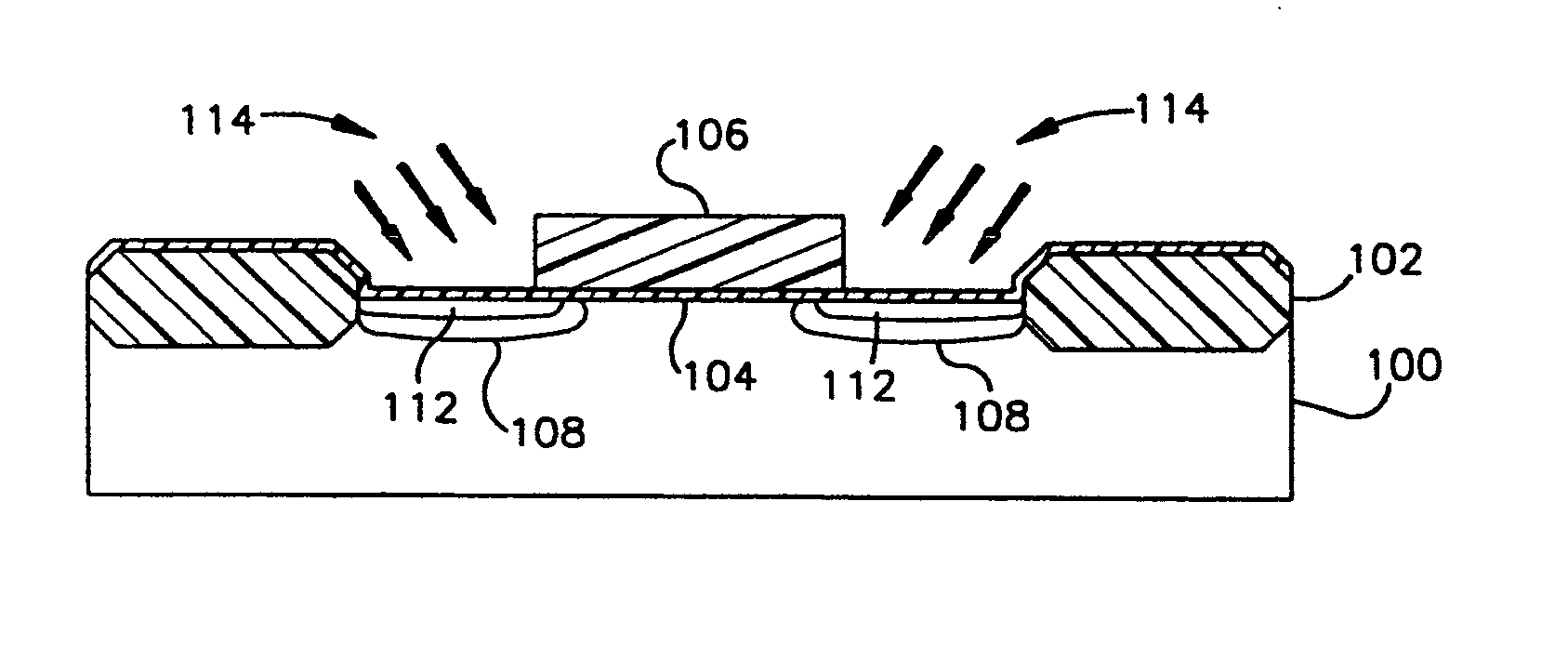
[0020]FIG. 1 depicts a schematic cross-sectional view of a transistor 10 in accordance with an aspect of the present invention. The transistor 10 can be a p-channel transistor or an n-channel transistor. For purposes of simplicity of explanation, the following discussion of FIG. 1 will assume an n-channel transistor, such as an NMOS. The transistor 10 includes a gate structure 12 that is disposed over a gate dielectric layer 14. To f...
PUM
 Abstract
Description
Claims
Application Information