

Photosensor and display device including photosensor
- Summary
- Abstract
- Description
- Claims
- Application Information
AI Technical Summary
Benefits of technology
Problems solved by technology
Method used
Image

Examples
Embodiment Construction
[0049] The present invention will be described more fully hereinafter with reference to the accompanying drawings, in which exemplary embodiments of the invention are shown.
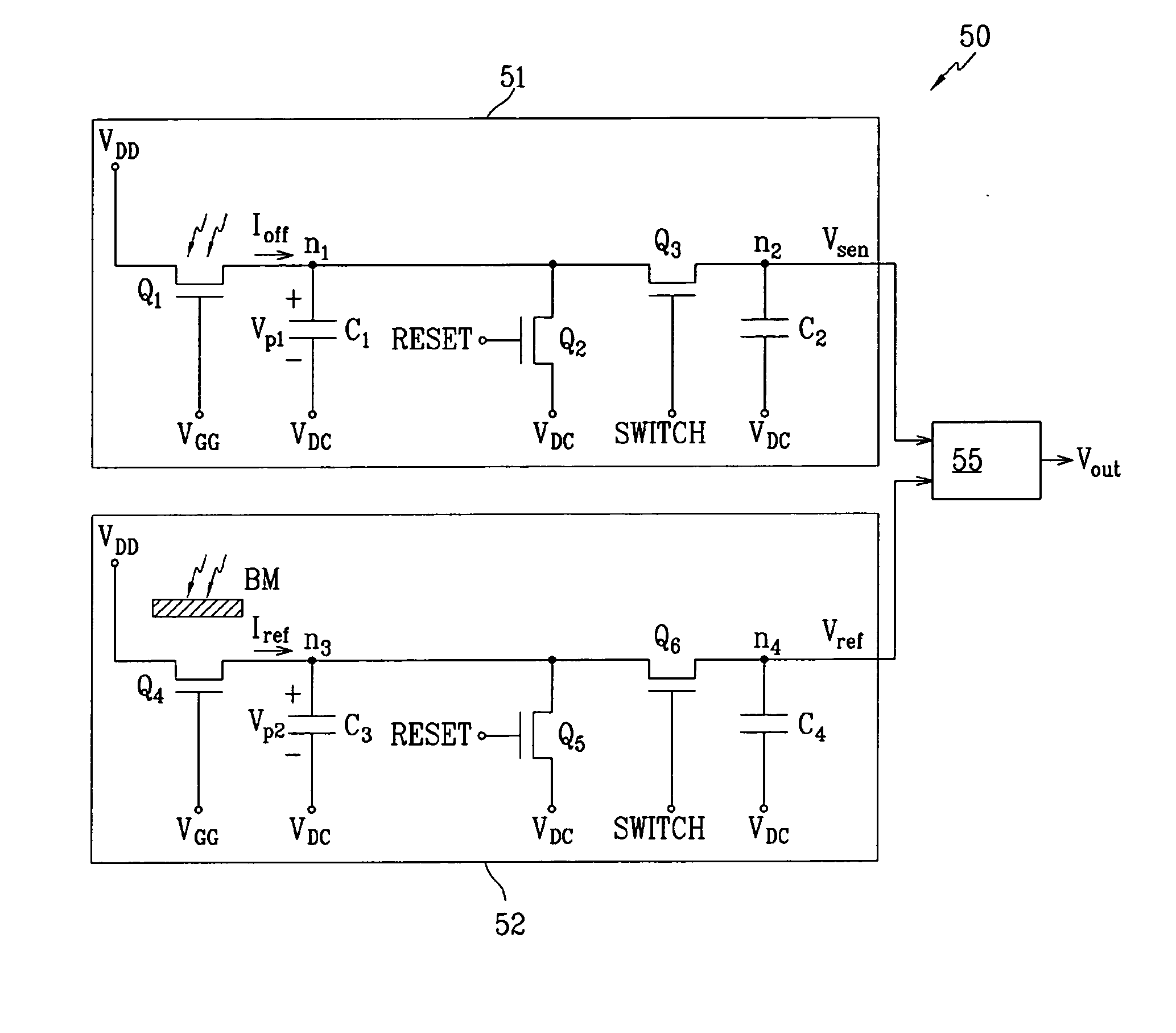
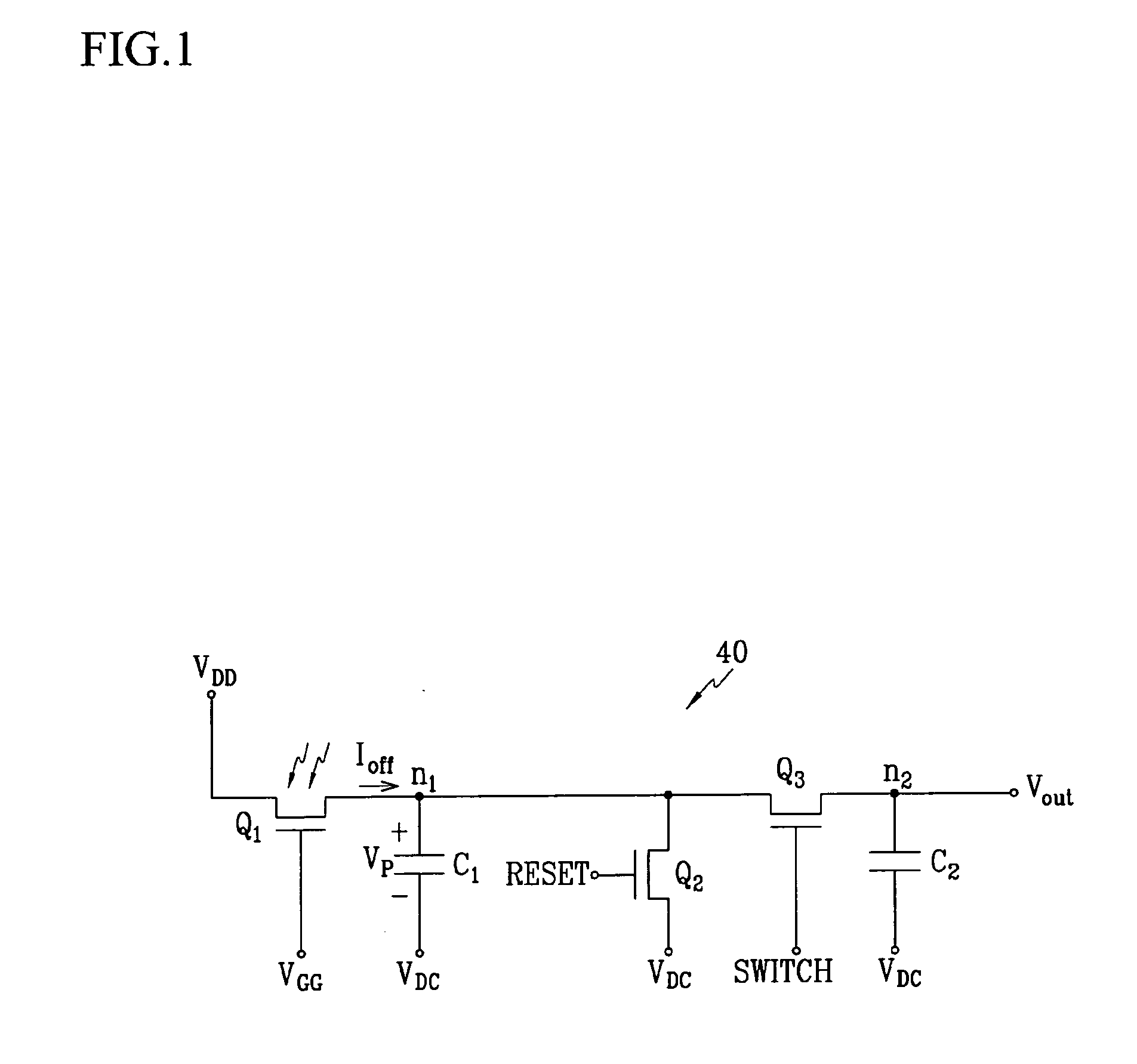
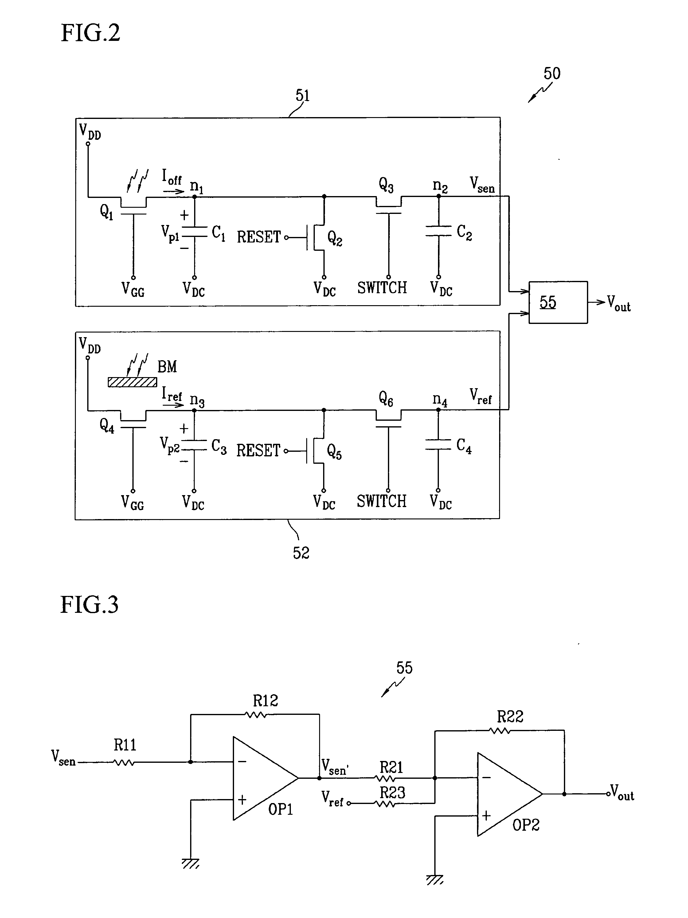
[0050] First, a photosensor according to an embodiment of the present invention will be described in detail with reference to FIG. 1. FIG. 1 is an equivalent circuit diagram of a photosensor according to an exemplary embodiment of the present invention.
[0051] As shown in FIG. 1, a photosensor 40 according to this exemplary embodiment of the present invention includes three thin film transistors (TFTs) and two capacitors C1 and C2. The three TFTs include a sensor transistor Q1, a reset transistor Q2 and a switching transistor Q3. The photosensor 40 generates a sensor output voltage Vout having a magnitude that varies in response to an amount of external light received.
[0052] The sensor transistor Q1 has a drain supplied with a first voltage VDD, a gate supplied with a second voltage VGG, and a source. The reset...
PUM
 Abstract
Description
Claims
Application Information