Nanofiber surface based capacitors

a surface based capacitor and nanofiber technology, applied in the field of nanotechnology, can solve the problems of limiting the effectiveness of such measures, affecting the efficiency or use of such devices, and affecting the efficiency of such measures, so as to achieve greater capacitance, greater surface area, and greater amount

Active Publication Date: 2005-10-06
ONED MATERIAL INC
View PDF39 Cites 91 Cited by
  • Summary
  • Abstract
  • Description
  • Claims
  • Application Information

AI Technical Summary

Benefits of technology

[0014] In yet other embodiments, the capacitors of the invention can comprise an electrode surface that, because of the nanofibers present, is considerably greater in surface area than other typical electrode surfaces of similar or substantially equal footprint. For example, the density of the members of the plurality of nanofibers can optionally increase the surface area of the electrode surface from at least 1.5 times to at least 100,00 times or more, at least 5 times to at least 75,000 times or more, at least 10 times to at least 50,000 times or more, at least 50 times to at least 25,000 times or more, at least 100 times to at least 10,000 times or more, or at least 500 times to at least 1,000 times or more, greater, in comparison to an area of substantially equal footprint of an electrode surface without nanofibers.

Problems solved by technology

In almost all instances, however, the efficiency or use of such devices is limited, at least in part, by the area of the surface which is in contact with, or comprises, the electrode plates of the capacitor.
First, space limitations (or “footprint” limitations) are of concern.
However, besides being inelegant, such response is often problematic due to cost restraints and size limitations imposed on the footprint itself (e.g., the capacitor might need to be placed in a limited space in a device, etc.)
While such porous matrices do increase the surface area of the electrode surface, a number of issues arise to limit the effectiveness of such measures.
A final, but not trivial, problem concerns cost.
Larger devices / surfaces / structures that are needed, e.g., to allow the proper capacitance, can be quite expensive.

Method used


Image

  • Nanofiber surface based capacitors
  • Nanofiber surface based capacitors
  • Nanofiber surface based capacitors

Examples


Embodiment Construction

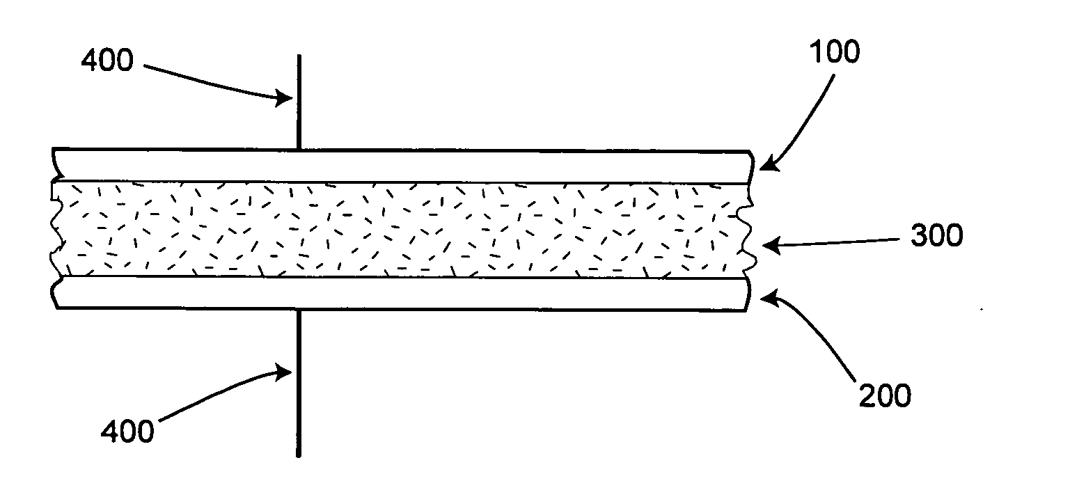
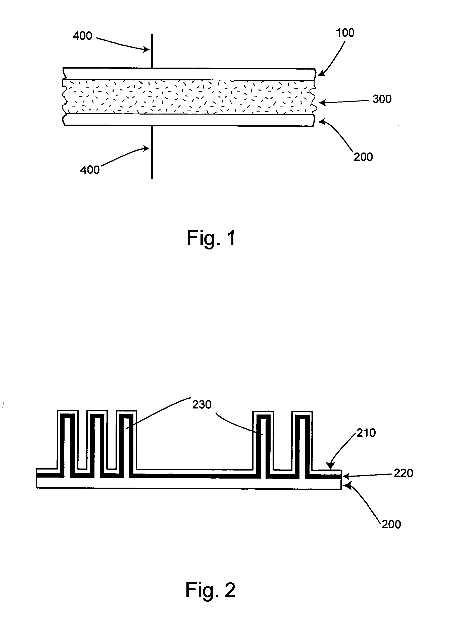
[0022] The current invention comprises a number of different embodiments focused on nanofiber enhanced area surface substrates and uses thereof in capacitors. As will be apparent upon examination of the present specification, figures, and claims, substrates having such enhanced surface areas present improved and unique capacitance aspects that are beneficial in a wide variety of applications ranging from materials science to medical use and beyond. It will be appreciated that enhanced surface areas herein are sometimes labeled as “nanofiber enhanced surface areas” or, alternatively depending upon context, as “nanowire enhanced surface areas,” etc.

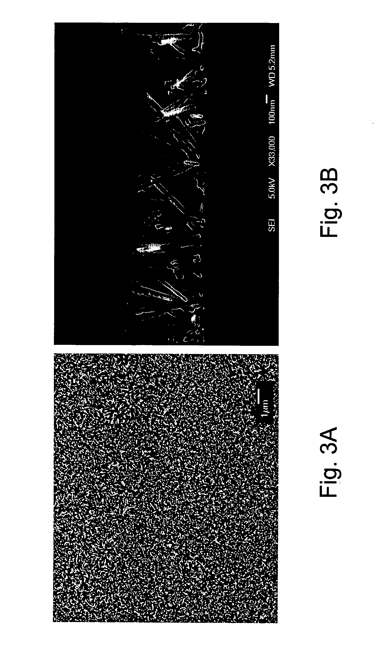
[0023] A common factor in the embodiments is the special morphology of nanofiber surfaces (typically silicon oxide nanowires herein, but also encompassing other compositions and forms). For example, the vastly increased surface area presented by such substrates is utilized in, e.g., creation of improved capacitors for a wide variety of use...


PUM


Abstract

This invention provides novel capacitors comprising nanofiber enhanced surface area substrates and structures comprising such capacitors, as well as methods and uses for such capacitors.

Description

CROSS-REFERENCE TO RELATED APPLICATIONS [0001] This application claims benefit of, and priority to, U.S. Provisional Application No. 60 / 554,549 filed Mar. 18, 2004. This prior application is hereby incorporated by reference in its entirety.FIELD OF THE INVENTION [0002] The invention relates primarily to the field of nanotechnology. More specifically, the invention pertains to capacitors comprising nanofibers and nanofiber enhanced surface areas, as well as to the use of such capacitors in various applications and devices. BACKGROUND OF THE INVENTION [0003] Various configurations of nanostructures (e.g., nanofibers, nanowires, nanocrystals, etc.) have attracted widespread interest for their novel properties in electrical, chemical, optical and other similar applications. Nanostructures have a broad possibility of uses, such as semiconductors for nanoscale electronics, optoelectronic applications (e.g., in lasers, LEDs, etc.) photovoltaics, sensors, etc. [0004] Correspondingly, capaci...

Claims


Application Information

Patent Timeline
Patent Type & Authority Applications(United States)
IPC IPC(8): H01G4/005H01G4/008H01G4/06H01G4/08
CPCH01G4/005H01G4/008H01G4/06H01G4/203Y02E60/13H01G9/04H01G11/36H01G11/46H01L28/82H01G4/33H05K1/162H05K2201/026
Inventor CHOW, CALVIN Y. H.DUBROW, ROBERT S.
Owner ONED MATERIAL INC
Why Eureka
Try Eureka