Dicing tape applying apparatus and back-grinding/dicing tape applying system

Inactive Publication Date: 2005-10-20
TOKYO SEIMITSU
View PDF4 Cites 34 Cited by
  • Summary
  • Abstract
  • Description
  • Claims
  • Application Information

AI Technical Summary

Benefits of technology

[0016] The present invention has been developed with the above-mentioned problems being taken into consideration, and the first object is to realize a dicing tape applying apparatus that can be used for both the non-cut dicing tape and the pre-cut dicing tape for

Problems solved by technology

Because of the fluidity, there is a problem that the adhesive may spread as far as an undesirable part.
For example, if the adhesive spreads to the surface of the die, the electric connection between the electrode pad and the connecting wire such as the bonding wire is adversely affected.
Conventionally, a die bonding tape is applied to each die one by one, but in this case the efficiency is insufficient and, therefore, a tape composed of a dicing tape and a die bonding tape bonded to each other is applied to the back of the wafer, and the wafer and the die bonding tape are cut together.
When a wafer is back-ground, distortions are produced and they are removed by etching, but etching cannot be performed in a state in which the protective tape is applied, therefore, etching is performed after the p

Method used


Image

  • Dicing tape applying apparatus and back-grinding/dicing tape applying system
  • Dicing tape applying apparatus and back-grinding/dicing tape applying system
  • Dicing tape applying apparatus and back-grinding/dicing tape applying system

Examples


Example

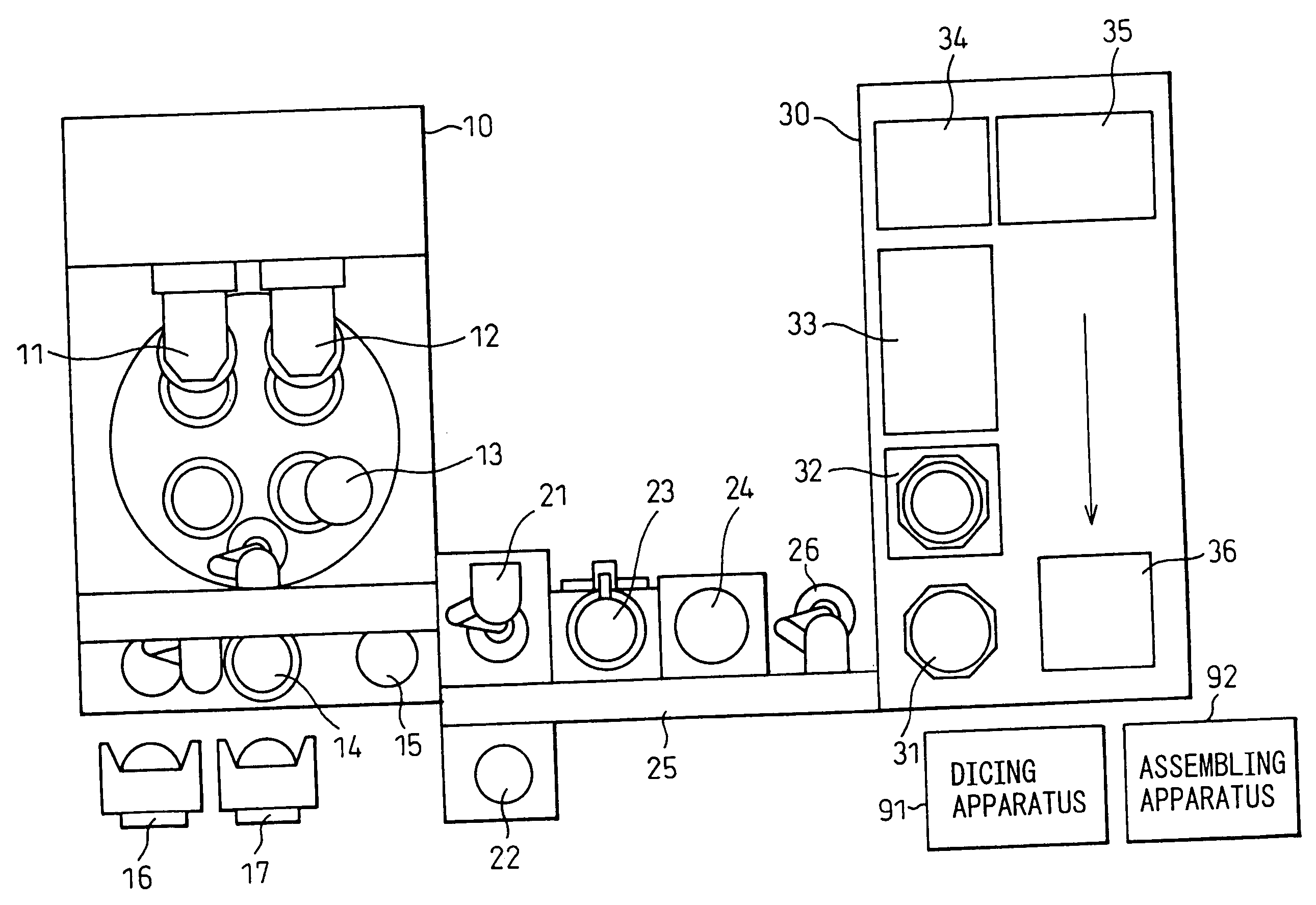
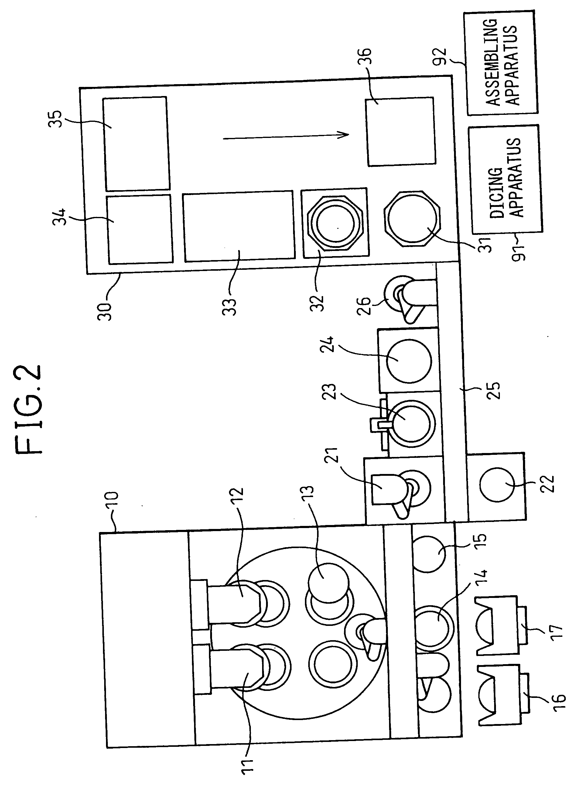
[0034]FIG. 2 is a diagram that shows the configuration of a polishing / back-grinding apparatus and a dicing tape applying apparatus in the embodiments of the present invention in the semiconductor manufacturing process.

[0035] As shown in FIG. 2, the wafer that has passed the probe test is supplied in a state of being contained in wafer cassettes 16 and 17. A protective tape is applied to the surface of the wafer. A robot arm of a polishing / back-grinding apparatus (PG) 10 takes out the wafer contained in the wafer cassettes 16 and 17 and conveys it onto the rotary table. As the table rotates, the wafer moves to a first grinder 11 and a second grinder and its back is polished (back-ground). Then, the wafer further moves to a polisher 13 and is polished to remove distortions. Then, the protective tapes on the back and surface of the wafer are cleaned by a cleaner 14 and the wafer is conveyed to a mounting base 15. A robot arm 21 conveys the thinned wafer on the mounting base 15 onto a ...


PUM


Abstract

A dicing tape applying apparatus, comprising a pre-cut dicing tape edge position detector detecting the edge of a pre-cut dicing tape and a cutter cutting a non-cut dicing tape into a desired shape when it is applied, and able to use both the non-cut dicing tape and the pre-cut dicing tape, has been disclosed.

Description

CROSS-REFERENCE-TO RELATED APPLICATION(S) [0001] This application is a divisional of U.S. application Ser. No. 10 / 613,492, filed Jul. 2, 2003, which claims priority of Japanese patent Application No. 2002-204704, filed Jul. 12, 2002, priority of which are claimed herein.BACKGROUND OF THE INVENTION [0002] The present invention relates to a dicing tape applying apparatus that applies a dicing tape to the back of a wafer before dicing and a back-grinding / dicing tape applying system that comprises a back-grinder that thins a wafer by grinding the back of the wafer and a dicing tape applying apparatus that applies a dicing tape to the back of the thinned wafer. [0003] In manufacturing semiconductors, after many chips (dice) are formed on the surface of a wafer, semiconductor chips are completed through a dicing process in which dice are separated and an assembling process in which they are fixed to a lead frame or the like and bonding is performed. In the dicing process, grooves are form...

Claims


Application Information

Patent Timeline
IPC IPC(8): H01L21/00H01L21/683H01L21/301H01L21/304
CPCH01L21/67132H01L21/6836H01L2221/68327Y10T29/41H01L2221/68386H01L2221/68395H01L2221/6834H01L21/304
Inventor KOBAYASHI, KAZUO
Owner TOKYO SEIMITSU
Why Eureka
Try Eureka