Manufacturing method for semiconductor device, semiconductor device and semiconductor chip
Active Publication Date: 2005-10-20
ROHM CO LTD +1
View PDF10 Cites 89 Cited by
Summary
Abstract
Description
Claims
Application Information
AI Technical Summary
This helps you quickly interpret patents by identifying the three key elements:
Problems solved by technology
Method used
Benefits of technology
Benefits of technology
[0031] Therefore, an object of this invention is to provide a manufacturing method for a semiconductor device where a short-circuiting defect is not easily generated by a connection member for connection to another semiconductor chip.
[0032] Another object of this invention is to provide a manufacturing method for a semiconductor device where cracking is not easily caused in a semiconductor chip.
Problems solved by technology
As a result of this, there is a risk that two rear surface side connection members 112 may be electrically short-circuited, causing a short-circuiting defect in the case where these rear surface side connection members 112 are placed in proximity.
There is a risk that short-circuiting defects will be caused by such deformations.
As a result of this, there is a risk that joining of semiconductor chip 103 to solid state device 102 or another semiconductor chip 103 may not be sufficiently achieved.
Method used
Image
Click on the blue label to locate the original text in one second.
Reading with bidirectional positioning of images and text.
Examples
first embodiment
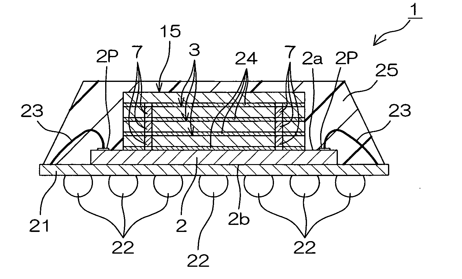
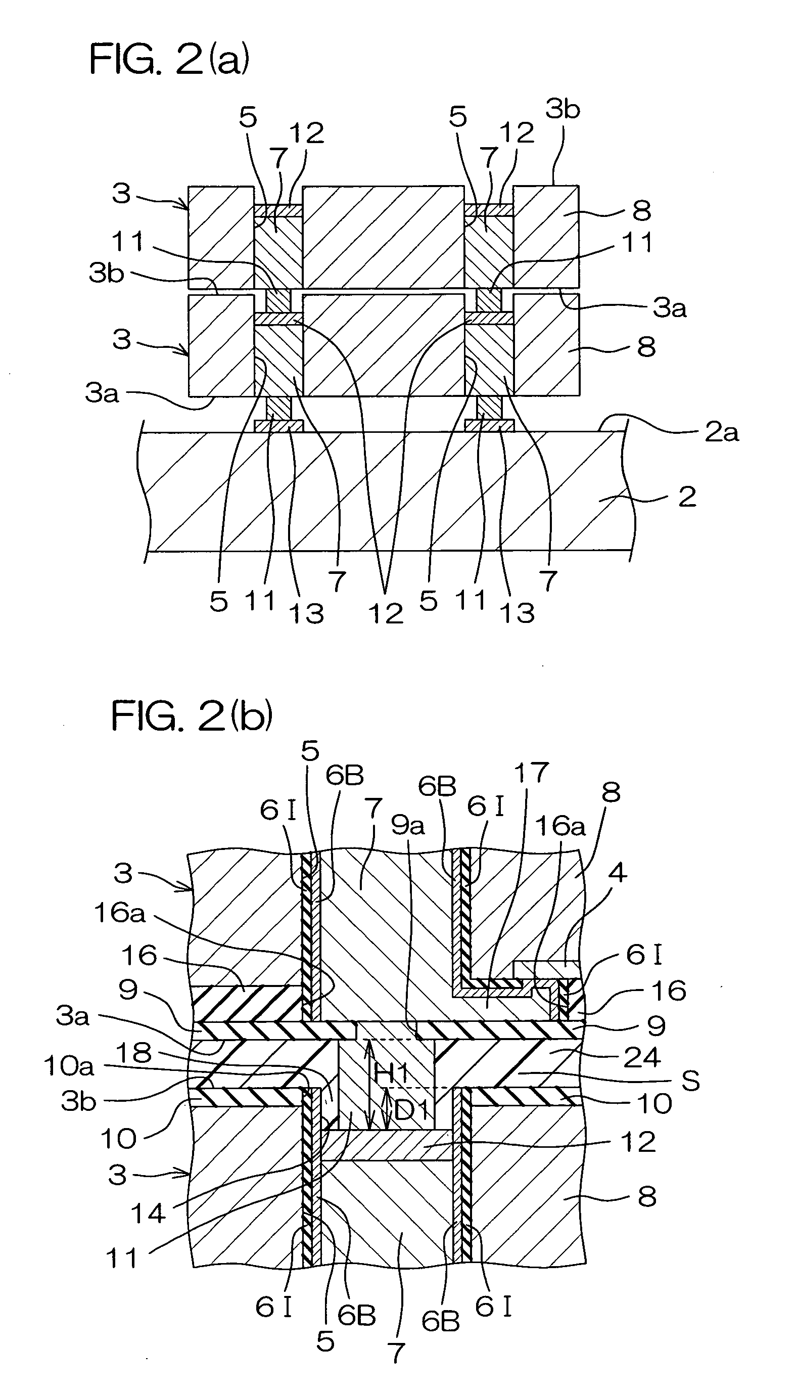
[0164]FIG. 1 is an illustrative cross sectional diagram showing the structure of a semiconductor device according to the present invention.
[0165] This semiconductor device 1 has a so-called BGA (ball grid array) type package form and a multi-chip stack structure, and is provided with a wiring substrate (an interposer) 21, a solid state device 2 such as a semiconductor chip or a wiring substrate, and semiconductor chips 3 and 15 which are in plate form and are stacked approximately parallel to each other, as well as metal balls 22.
[0166] Wiring substrate 21 is made of an insulator and wires are provided on the surfaces and / or inside thereof. Solid state device 2, a plurality of (three in this embodiment) semiconductor chips 3 having feedthrough electrodes 7, semiconductor chip 15 which does not have feedthroughelectrode 7 are sequentially stacked on one surface side of wiring substrate 21. Metal balls (for example, solder balls) 22 are joined to the other surface (surface on the si...
second embodiment
[0263]FIG. 7(a) and FIG. 7(b) are illustrative cross sectional diagrams showing the structure of a semiconductor device according to the present invention. In FIG. 7(a) and FIG. 7(b), the same reference symbols as in FIG. 1, FIG. 2(a) and FIG. 2(b) are attached to parts that correspond to the respective parts shown in FIG. 1, FIG. 2(a) and FIG. 2(b), and overlapping descriptions thereof are omitted. FIG. 7(a) shows the entirety of this semiconductor device, and FIG. 7(b) shows an area in the vicinity of a portion where two semiconductor chips are adjacent to each other in an enlarged manner.
[0264] In reference to FIG. 7(a), this semiconductor device 41 is provided with three semiconductor chips 43, 44 and 45, which are sequentially placed from the solid state device 2 side instead of the three semiconductor chips 3 of semiconductor device 1 shown in FIG. 1, FIG. 2(a) and FIG. 2(b). Semiconductor chips 43, 44 and 45 respectively have feedthrough electrodes 47, 48 and 49. Feedthrough ...
third embodiment
[0284]FIG. 10 is an illustrative cross sectional diagram showing the structure of a semiconductor device according to the present invention. In FIG. 10, the same reference symbols as those in FIG. 1, FIG. 2(a) and FIG. 2(b) are attached to parts that correspond to the respective parts shown in FIG. 1, FIG. 2(a) and FIG. 2(b), and descriptions thereof are omitted.
[0285] This semiconductor device 51 has a structure which is similar to that of semiconductor device 1 shown in FIG. 1, FIG. 2(a) and FIG. 2(b) and is provided with semiconductor chips 53 instead of semiconductor chips 3.
[0286] Semiconductor chip 53 has a structure which is similar to that of semiconductor chip 3 and a resin material layer 55 is formed on rear surface protective film 10. Although it is preferable for resin material layer 55 to be made of a fluorine resin (tetrafluoroethylene resin) or polyimide, resin material layer 55 may be made of an epoxy based resin, an acryl based resin, or the like. In addition, in t...
PUM
Abstract
A manufacturing method for a semiconductor device includes: the step of preparing a semiconductorchip which is provided with a functional element formed on a front surface side of a semiconductor substrate, a feedthroughelectrode which is placed within a through hole that penetrates the semiconductor substrate, a front surface side connection member which protrudes from the front surface, and a rear surface side connection member which has a joining surface within a recess that is formed in a rear surface; the step of preparing a solid state device where a solid state device side connection member for connection to the front surface side connection member is formed on one surface; and the joining step of making the front surface of the semiconductor chip face the first surface of the solid state device by holding the rear surface of the semiconductor chip, and of joining the front surface side connection member to the solid state device side connection member.
Description
BACKGROUND OF THE INVENTION [0001] 1. Field of the Invention [0002] This invention relates to a semiconductor device having a multi-chip stack structure, where a solid state device and one or more semiconductor chips are stacked and joined, and a manufacturing method for the same, as well as a semiconductor chip which is used in such a manufacturing method. [0003] 2. Description of Related Art [0004] A semiconductor device having a multi-chip stack structure where one or more semiconductor chips are stacked on the surface of a solid state device such as a semiconductor chip or a wiring substrate has been conventionally known. [0005]FIG. 30(a) and FIG. 30(b) are illustrative cross sectional diagrams showing the structure of a conventional semiconductor device having a multi-chip stack structure. A semiconductor device having such a structure is disclosed in, for example, “Proceedings of the 2003 VMIC (VLSI Multi-Level Interconnection) Conference,” M. Hoshino et al., September 2003, p...
Claims
Application Information
Patent Timeline
Application Date:The date an application was filed.
Publication Date:The date a patent or application was officially published.
First Publication Date:The earliest publication date of a patent with the same application number.
Issue Date:Publication date of the patent grant document.
PCT Entry Date:The Entry date of PCT National Phase.
Estimated Expiry Date:The statutory expiry date of a patent right according to the Patent Law, and it is the longest term of protection that the patent right can achieve without the termination of the patent right due to other reasons(Term extension factor has been taken into account ).
Invalid Date:Actual expiry date is based on effective date or publication date of legal transaction data of invalid patent.

