Method and apparatus for using light emitting diodes

a technology of light-emitting diodes and methods, applied in the field of light-emitting diodes, can solve the problems of affecting the ability to concentrate higher power levels into smaller packages, affecting the reliability of the device, and affecting the ability to control the power level of the device,

Inactive Publication Date: 2005-10-20
KONINKLIJKE PHILIPS ELECTRONICS NV
View PDF99 Cites 226 Cited by
  • Summary
  • Abstract
  • Description
  • Claims
  • Application Information

AI Technical Summary

Benefits of technology

[0019] In a tenth embodiment, the present invention is a device comprising a first circuit layer having a first aperture and a conductive heat spreader layer. The heat spreader is receivable within the aperture of the first circuit layer. At least one light emitting device is secured to the heat spreader layer. A second circuit layer is mounted on the first circuit layer with the second circuit layer having a second aperture for receiving each light emitting device. Circuit traces are formed on the second circuit layer and means for connecting the circuit traces to each light emitting device.

Problems solved by technology

Heat can damage sensitive electronic components, degrading reliability and hampering the ability to concentrate higher power levels into smaller packages.
Many applications would benefit from the ability to closely package LEDs into compact configurations, but the heat levels generated have always been a limiting factor.
As LEDs become more sophisticated, eliminating internal heat build-up has also become increasingly difficult.
Devices are becoming more powerful and creating solutions for removing the resulting heat generation often pose great challenges.
High current densities within the junction of the chip cause partial overheating which damages the crystalline structure of the LED die.
It is believed that none of these U.S. patent documents disclose LEDs on the tips of heat pipes and cooling in a manner to dissipate internal heat energy and packaging the same to achieve maximum light output.

Method used


Image

  • Method and apparatus for using light emitting diodes
  • Method and apparatus for using light emitting diodes
  • Method and apparatus for using light emitting diodes

Examples


Embodiment Construction

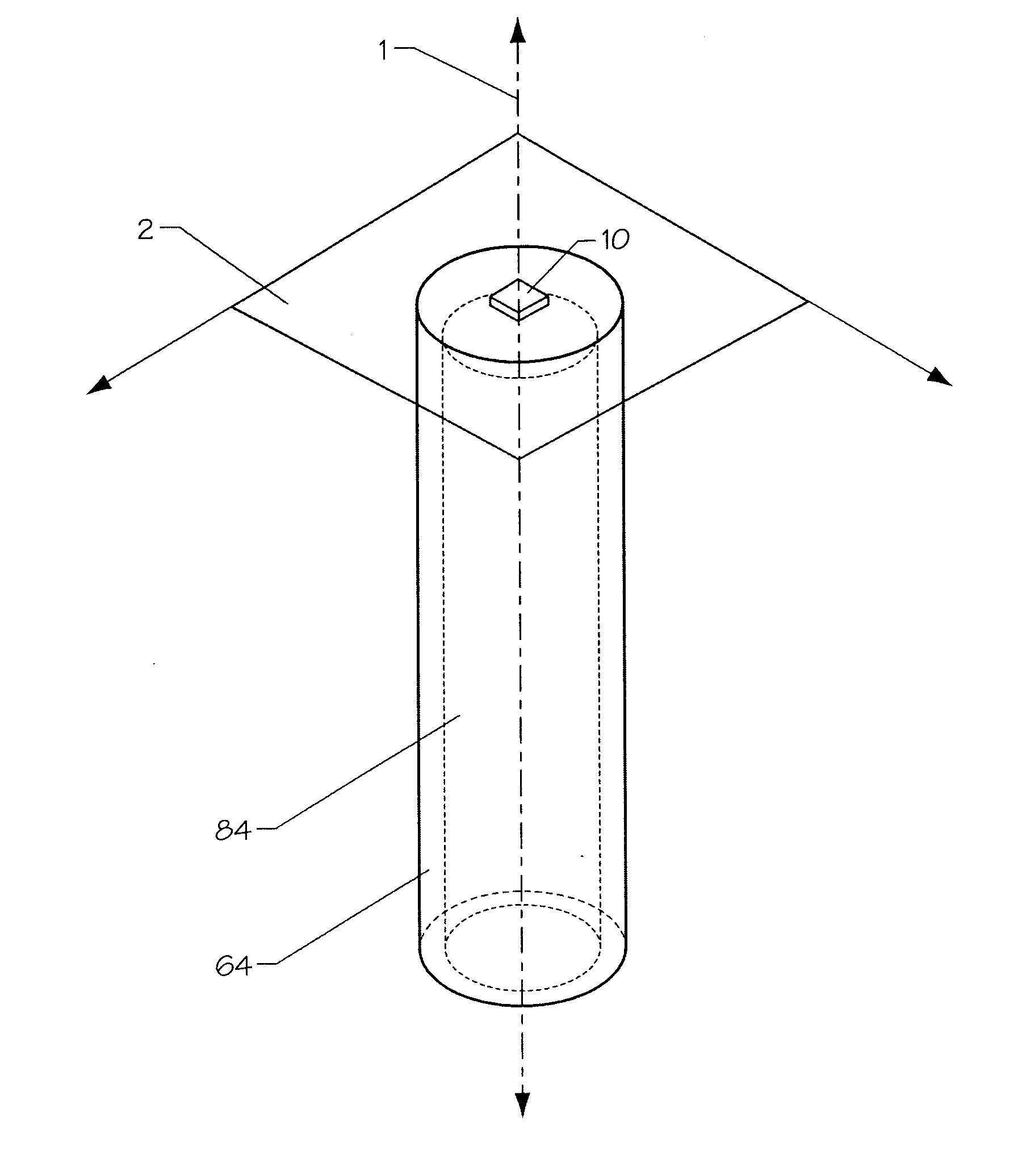
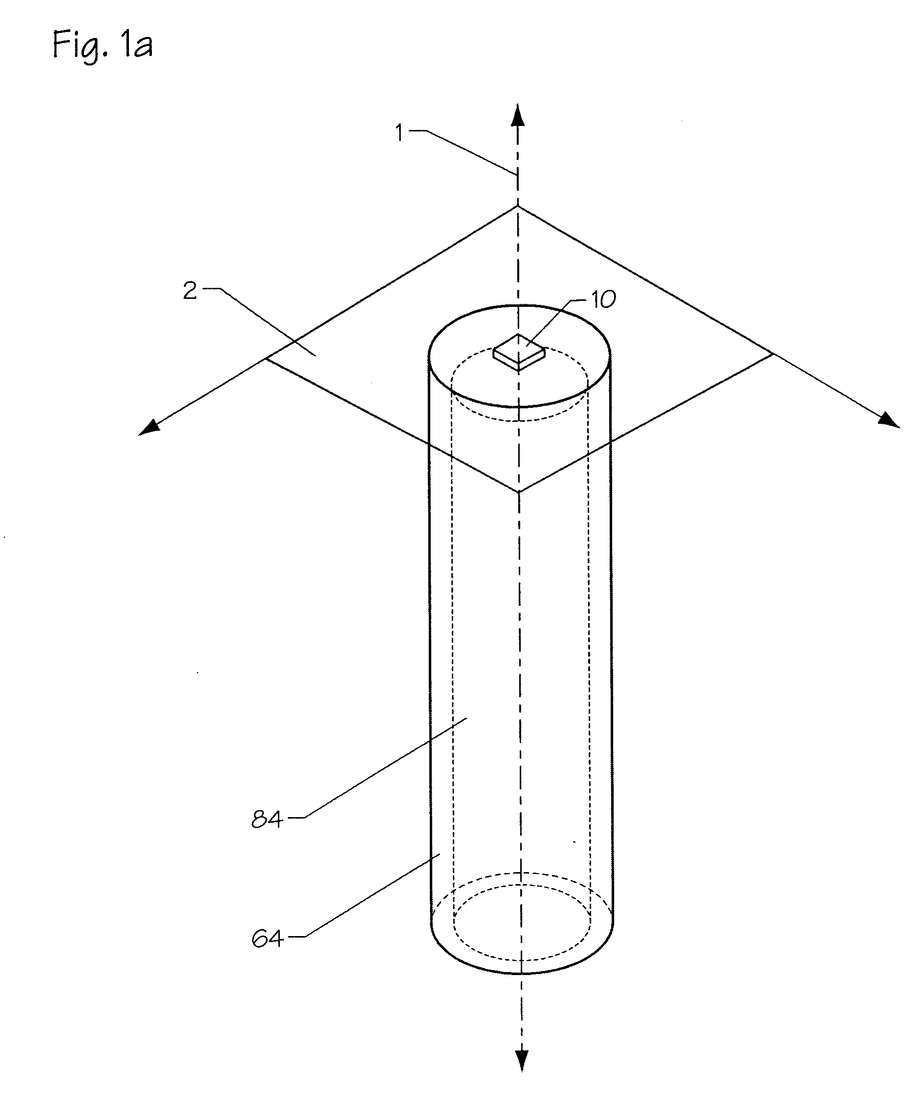
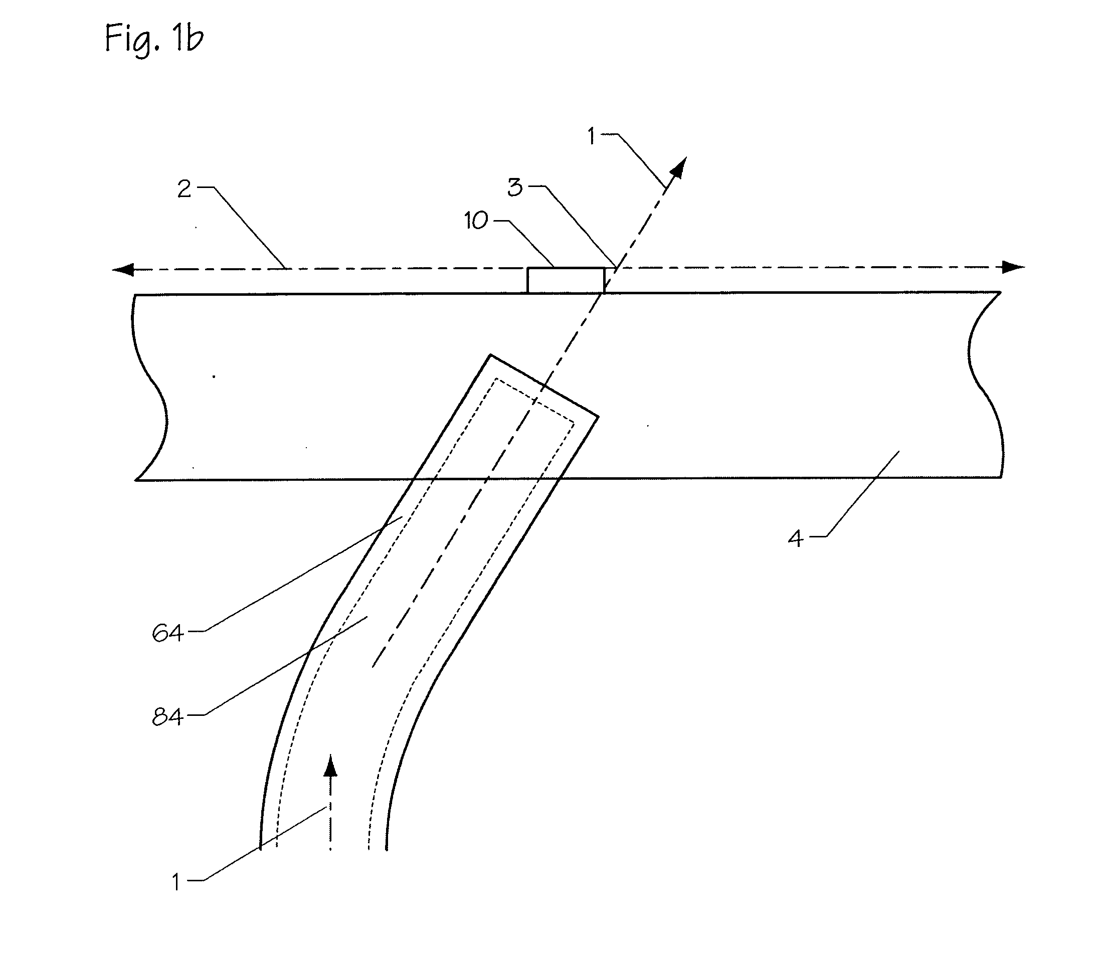
[0090] The present invention provides high power LEDs and heat pipe technology which allows for ultra-high power density packaging. The ultra-high thermal conductivity of the heat pipe allows for over-driving the LEDs by a factor of 4×, while maintaining junction temperatures well within rated limits. Other attributes include low thermal resistance submount brightness-maintaining TIR reflector, low cross-sectional area heat sink, and individually addressable high-density chip array. These attributes facilitate the ability to achieve high power densities, even without integral heat pipes, which is especially useful for those applications that do not demand ultra-high thermal performance.

[0091] The manner of bonding of the LED device to the heat pipe component as in the present invention minimizes the physical space requirements while taking advantage a pipes' unique rapid heat dissipation capabilities. This allows much more closely spaced LEDs operating at higher power and brightnes...


PUM


Abstract

The present invention provides a method and apparatus for using light emitting diodes for curing and various solid state lighting applications. The method includes a novel method for cooling the light emitting diodes and mounting the same on heat pipe in a manner which delivers ultra high power in UV, visible and IR regions. Furthermore, the unique LED packaging technology of the present invention utilizes heat pipes that perform very efficiently in very compact space. Much more closely spaced LEDs operating at higher power levels and brightness are possible because the thermal energy is transported in an axial direction down the heat pipe and away from the light-emitting direction rather than a radial direction in nearly the same plane as the “p-n” junction.

Description

CROSS REFERENCE TO RELATED APPLICATIONS: [0001] This application claims benefit of priority of U.S. Provisional Application No. 2002; 60 / 405,432, filed Aug. 23, 2002; Ser. No. 60 / 410,720, filed Sep. 13, 2002; Ser. No. 60 / 418,948, filed Oct. 8, 2002; Ser. No. 60 / 420,479, filed Oct. 22, 2002; Ser. No. 60 / 467,702, filed May 3, 2003 and Ser. No. 60 / 476,004, filed on Jun. 4, 2003.FIELD OF THE INVENTION [0002] This invention relates to the field of light emitting diode (“LED”) technology, particularly to improvement in light-emitting devices by integration of novel packaging methodologies to make much higher output LED devices. BACKGROUND OF THE INVENTION [0003] Heat can damage sensitive electronic components, degrading reliability and hampering the ability to concentrate higher power levels into smaller packages. Many applications would benefit from the ability to closely package LEDs into compact configurations, but the heat levels generated have always been a limiting factor. As LEDs b...

Claims


Application Information

Patent Timeline
Patent Type & Authority Applications(United States)
IPC IPC(8): A61C3/00A61C13/15A61C19/00A61C19/06H01L25/13H01L33/64
CPCA61C19/003A61C19/004H01L2924/1461H01L2924/3025H01L2924/3011H01L2224/73265H01L2224/48091H05K2201/10106H05K1/0209A61C19/066F28D15/02H01L33/648F21V29/006H05K1/0203H01L2924/00014H01L2924/00H01L2924/12044F21V29/51F21K9/23F21Y2115/10H01L33/00
Inventor DAHM, JONATHAN S.
Owner KONINKLIJKE PHILIPS ELECTRONICS NV
Why Eureka
Try Eureka