

NAND flash memory device and method of programming the same
a technology of flash memory and programming method, which is applied in the direction of digital storage, static storage, instruments, etc., can solve the problems of more program disturbance in the cell, more voltage difference between gate and channel,
- Summary
- Abstract
- Description
- Claims
- Application Information
AI Technical Summary
Problems solved by technology
Method used
Image

Examples
first embodiment
[0032]FIG. 3 is a schematic diagram illustrating a method of programming the NAND flash memory device in accordance with the present invention.
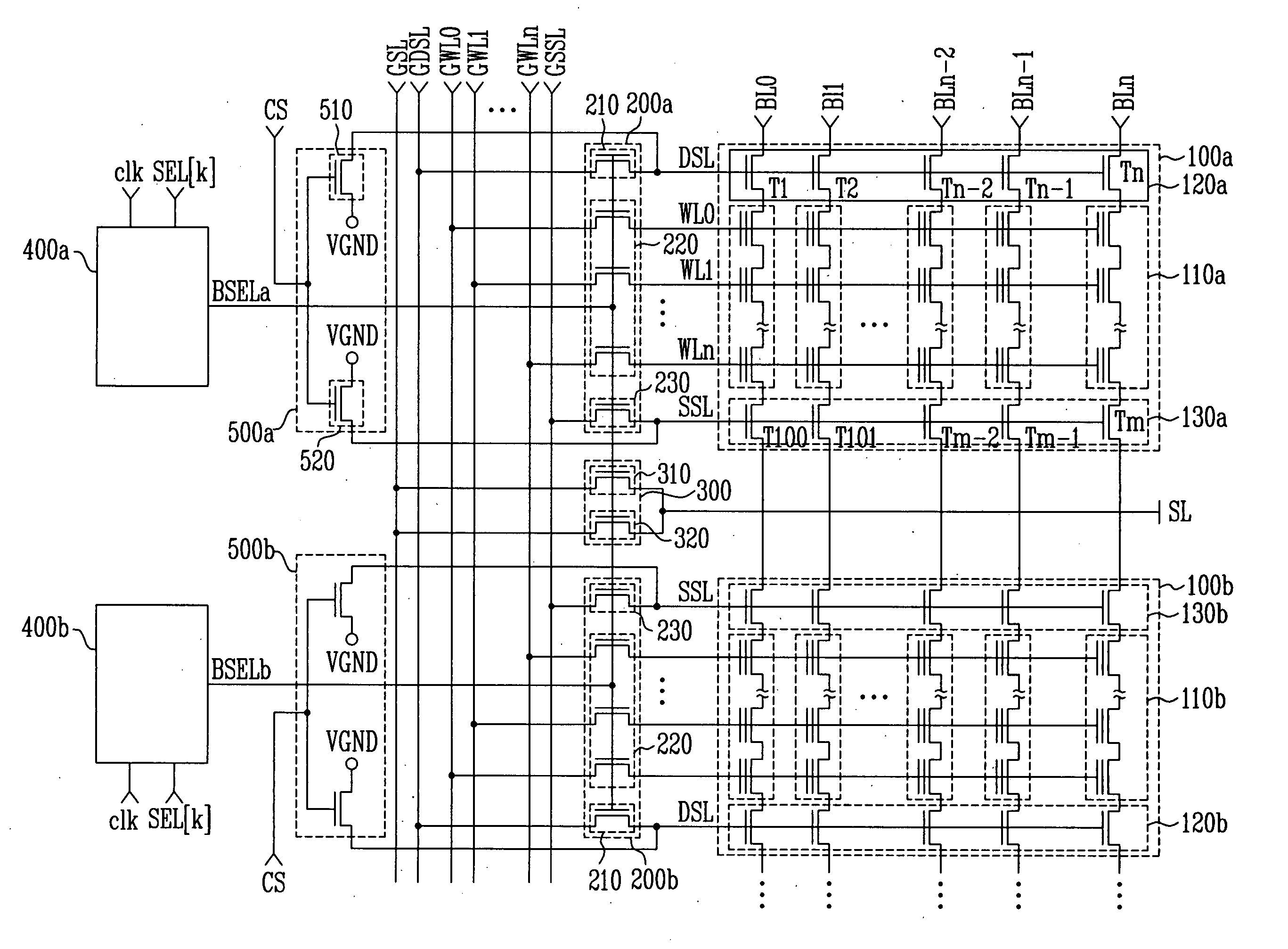
[0033] Referring to FIGS. 1 and 3, in a method of programming the NAND flash memory device, including: a plurality of cell blocks 100 having a plurality of cell strings 110 connected with a plurality of cell in series, a plurality of string select transistors T1 to Tn connected with a drain terminal of the cell string, and a plurality of source select transistors T100 to Tm connected with a source terminal of the cell string 110; a plurality of bitlines BL0 to BLn connected respectively with a drain terminal of the plurality of string select transistors T1 to Tn and a string select line DSL connected a gate terminal; a source line connected with a source terminal of the plurality of source select transistors T100 to Tm and a source select line SSL connected with the gate terminal; word lines WL0 to WLn connected with each gate terminal of the...
second embodiment
[0039]FIG. 4 is a schematic diagram illustrating a method of programming a NAND flash memory device in accordance with the present invention.
[0040] Referring to FIGS. 1 and 4, in a method of programming the NAND flash memory device, including: a plurality of cell blocks 100 having a plurality of cell strings 110 connected with a plurality of cell in series, a plurality of string select transistors T1 to Tn connected with a drain terminal of the cell string, and a plurality of source select transistors T100 to Tm connected with a source terminal of the cell string 110; a plurality of bitlines BL0 to BLn connected respectively with a drain terminal of the plurality of string select transistors T1 to Tn and a string select line DSL connected a gate terminal; a source line connected with a source terminal of the plurality of source select transistors T100 to Tm and a source select line SSL connected with the gate terminal; word lines WL0 to WLn connected with each gate terminal of the p...
third embodiment
[0048]FIG. 5 is a schematic diagram illustrating a method of programming a NAND flash memory device in accordance with the present invention.
[0049] Referring to FIGS. 1 and 5, in a method of programming the NAND flash memory device, including: a plurality of cell blocks 100 having a plurality of cell strings 10 connected with a plurality of cells in series, a plurality of string select transistors T1 to Tn connected with a drain terminal of the cell string, and a plurality of source select transistors T100 to Tm connected with a source terminal of the cell string 110; a plurality of bitlines BL0 to BLn connected respectively with a drain terminal of the plurality of string select transistors T1 to Tn and a string select line DSL connected a gate terminal; a source line connected with a source terminal of the plurality of source select transistors T100 to Tm and a source select line SSL connected with the gate terminal; word lines WL0 to WLn connected with each gate terminal of the p...
PUM
 Abstract
Description
Claims
Application Information