Device transfer method and display apparatus

a technology of device transfer and display apparatus, which is applied in the direction of identification means, instruments, semiconductor devices, etc., can solve the problems of difficult stripping of the device holding the substrate and the apparatus substrate from each other, damage to the substrate, and difficulty in transferring the device onto the apparatus substrate, so as to reduce the possibility of damage to the substrate. , the effect of easy stripping

Inactive Publication Date: 2005-10-20
SONY CORP
View PDF12 Cites 173 Cited by
  • Summary
  • Abstract
  • Description
  • Claims
  • Application Information

AI Technical Summary

Benefits of technology

[0008] The present invention provides in an embodiment a device transfer method and a display apparatus by or in which, in transferring devices arranged on a substrate onto another substrate, it is possible to easily strip the substrate after the transfer of the devices, to lower the possibility of damaging of the substrates, and to retransfer additional devices onto the same substrate after the transfer of the devices.

Problems solved by technology

For example, in such image display apparatuses as LCD and PDP, device separation is not possible, so that the individual devices generally are formed at intervals corresponding to the pixel pitch of the desired image display apparatus, from the beginning of the manufacturing process.
In this case, the device holding substrate and the apparatus substrate are adhered to each other, and then the device holding substrate and the apparatus substrate are stripped from each other; in this process, it is difficult to strip the device holding substrate and the apparatus substrate from each other, due to the strong adhesion therebetween by the adhesive.
Particularly, in the case of lamination of substrates having large areas, it is highly possible that the substrates may be damaged at the time of stripping.
Furthermore, since the adhesive layer is hardened (cured) in the condition where the devices are embedded in the adhesive layer, it is difficult to transfer the devices onto the apparatus substrate and thereafter again transfer devices onto the same apparatus substrate.

Method used


Image

  • Device transfer method and display apparatus
  • Device transfer method and display apparatus
  • Device transfer method and display apparatus

Examples


Embodiment Construction

[0039] The present invention relates to a device transfer method and a display apparatus. More particularly, the present invention relates to a device transfer method and a display apparatus by or in which devices can be transferred accurately.

[0040] The device transfer method and the display apparatus according to various embodiments of the present invention will be described in detail below, referring to the drawings Where it should be appreciated that the present invention is not limited to the following description, and modifications can be appropriately made without departure from the scope of the gist of the invention.

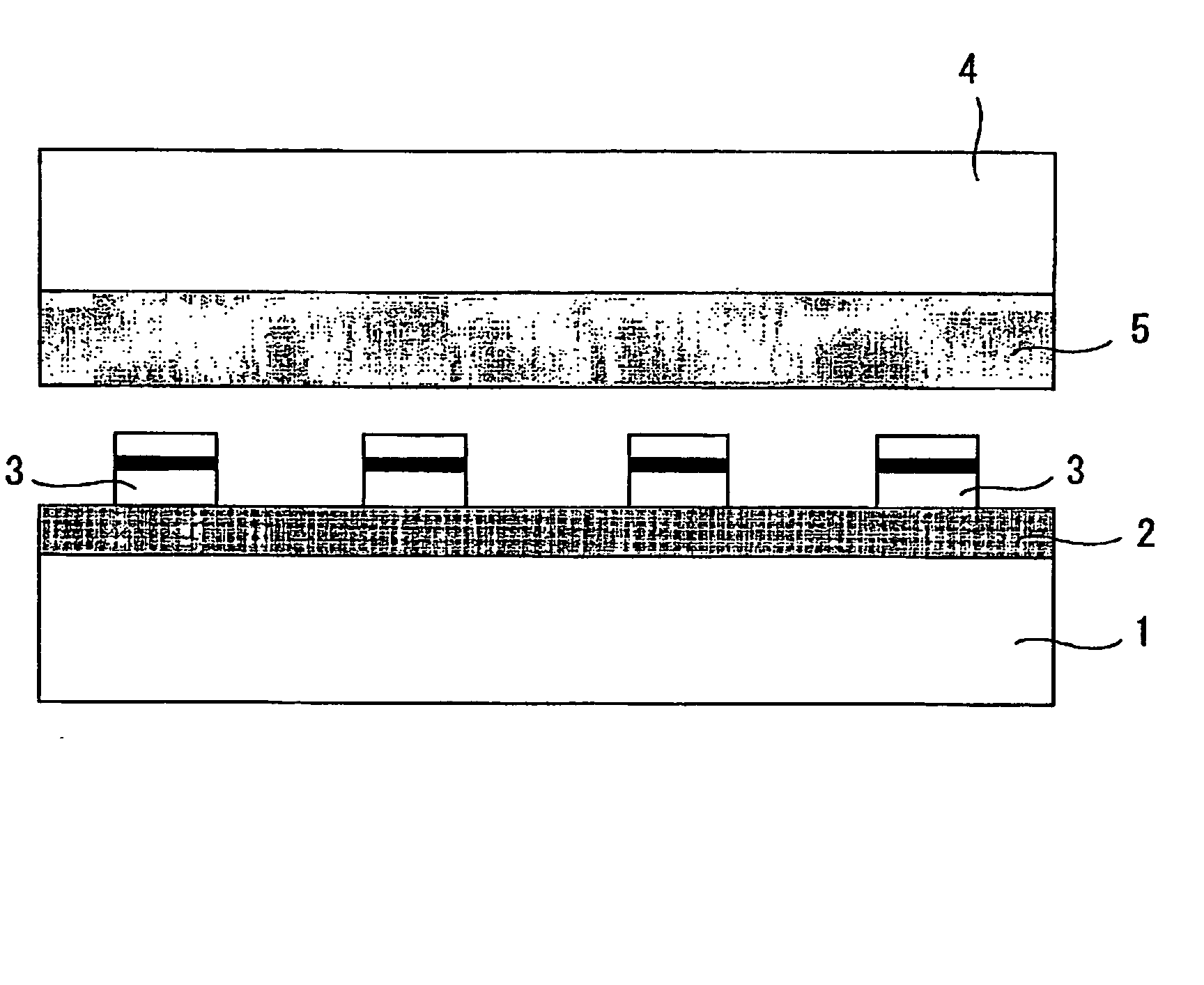
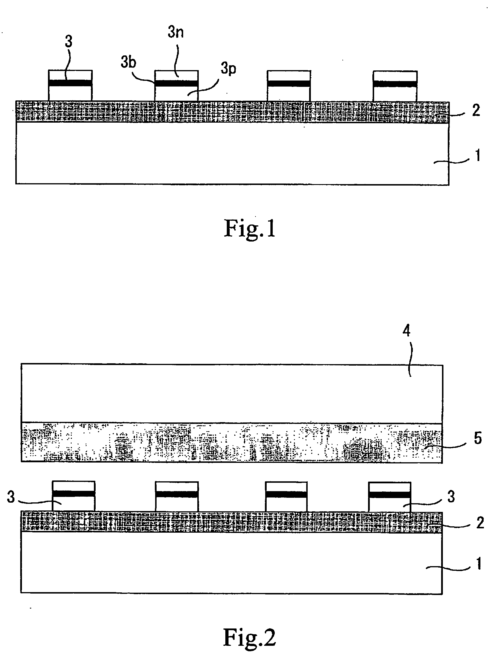
[0041] As shown in FIG. 1, a temporary adhesion layer 2 is formed on a temporary holding substrate 1, and devices 3 which are light-emitting diodes are arranged on the temporary adhesion layer 2. The temporary holding substrate 1 is a substrate having a desired rigidity, and various substrates such as semiconductor substrates, quartz glass substrates, plastic s...


PUM

PropertyMeasurementUnit
pressureaaaaaaaaaa
pressure sensitiveaaaaaaaaaa
areasaaaaaaaaaa

Abstract

A device transfer method and a display apparatus are provided. A device transfer method and a display apparatus are provided by or in which, in transferring devices arranged on a substrate onto another substrate, it is possible to easily strip the substrate after the transfer of the devices, to lower the possibility of damaging of the substrate, and to additionally transfer devices onto the same substrate after the transfer of the devices. A plurality of devices arranged on a temporary holding substrate are embedded into and held in a pressure sensitive adhesive layer formed on a transfer substrate, and the devices are stripped from the temporary holding substrate. Other devices are further additionally embedded into the pressure sensitive adhesive layer before hardening the pressure sensitive adhesive layer, whereby the devices can be arranged on a transfer substrate having a large area. Besides, where the devices additionally embedded into the pressure sensitive adhesive layer are different in characteristics from the devices embedded in the pressure sensitive adhesive layer in advance, it is possible to easily obtain a display apparatus for multicolor display, a display apparatus having a driving circuit, and the like.

Description

CROSS REFERENCES TO RELATED APPLICATIONS [0001] The present application claims priority to Japanese Patent Document No. P2003-059540 filed on Mar. 6, 2003, the disclosure of which is herein incorporated by reference. BACKGROUND OF THE INVENTION [0002] The present invention relates to a device transfer method and a display apparatus. More particularly, the present invention relates to a device transfer method and a display apparatus by or in which devices can be transferred accurately. [0003] In the case of assembling an image display apparatus by arranging light-emitting devices in a matrix, it has been a general practice to form the devices directly on a substrate as in the cases of liquid crystal displays (LCD) and plasma display panels (PDP) or to arrange singular light-emitting diode (LED) packages as in the case of light-emitting diode displays (LED displays). For example, in such image display apparatuses as LCD and PDP, device separation is not possible, so that the individua...

Claims


Application Information

Patent Timeline
Patent Type & Authority Applications(United States)
IPC IPC(8): G02F1/1343G09F9/00H01L21/60G02F1/13H01L21/68H01L25/075H01L33/32H01L33/48
CPCH01L21/6835H01L2924/12041H01L24/82H01L25/0753H01L2221/68368H01L2224/24226H01L2924/01004H01L2924/01013H01L2924/01015H01L2924/01018H01L2924/01033H01L2924/01039H01L2924/01052H01L2924/01075H01L2924/01079H01L2924/01005H01L2924/01006H01L2924/01019H01L2924/01047H01L2924/01076H01L24/24H01L2924/12042H01L2924/00G02F1/13
Inventor DOI, MASATOTOMODA, KATSUHIROWATANABE, TOSHIHIKOOOHATA, TOYOHARU
Owner SONY CORP
Why Eureka
Try Eureka