A semiconductor device and a manufacturing method thereof

A manufacturing method and semiconductor technology, applied in the fields of semiconductor/solid-state device manufacturing, semiconductor devices, semiconductor/solid-state device components, etc., can solve the problems of peeling, being easily affected by moisture, low mechanical strength, etc., and achieve the effect of improving peeling.

Inactive Publication Date: 2009-10-07
TERAMIKROS INC
View PDF1 Cites 29 Cited by
  • Summary
  • Abstract
  • Description
  • Claims
  • Application Information

AI Technical Summary

Problems solved by technology

[0006] However, in the semiconductor device provided with the above-mentioned low dielectric constant film, especially the porous type low dielectric constant film having a hollow structure, there are disadvantages such as low mechanical strength, easy to be affected by moisture, and easy to be damaged from the base. The problem of bottom stripping

Method used


Image

  • A semiconductor device and a manufacturing method thereof
  • A semiconductor device and a manufacturing method thereof
  • A semiconductor device and a manufacturing method thereof

Examples


no. 1 approach

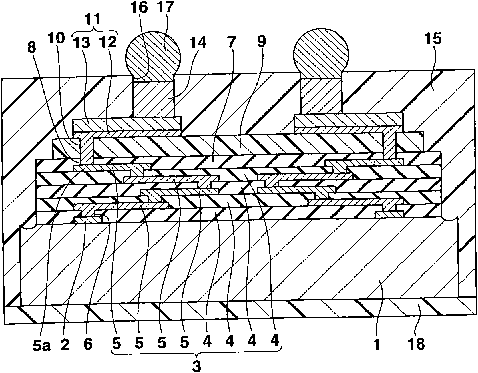
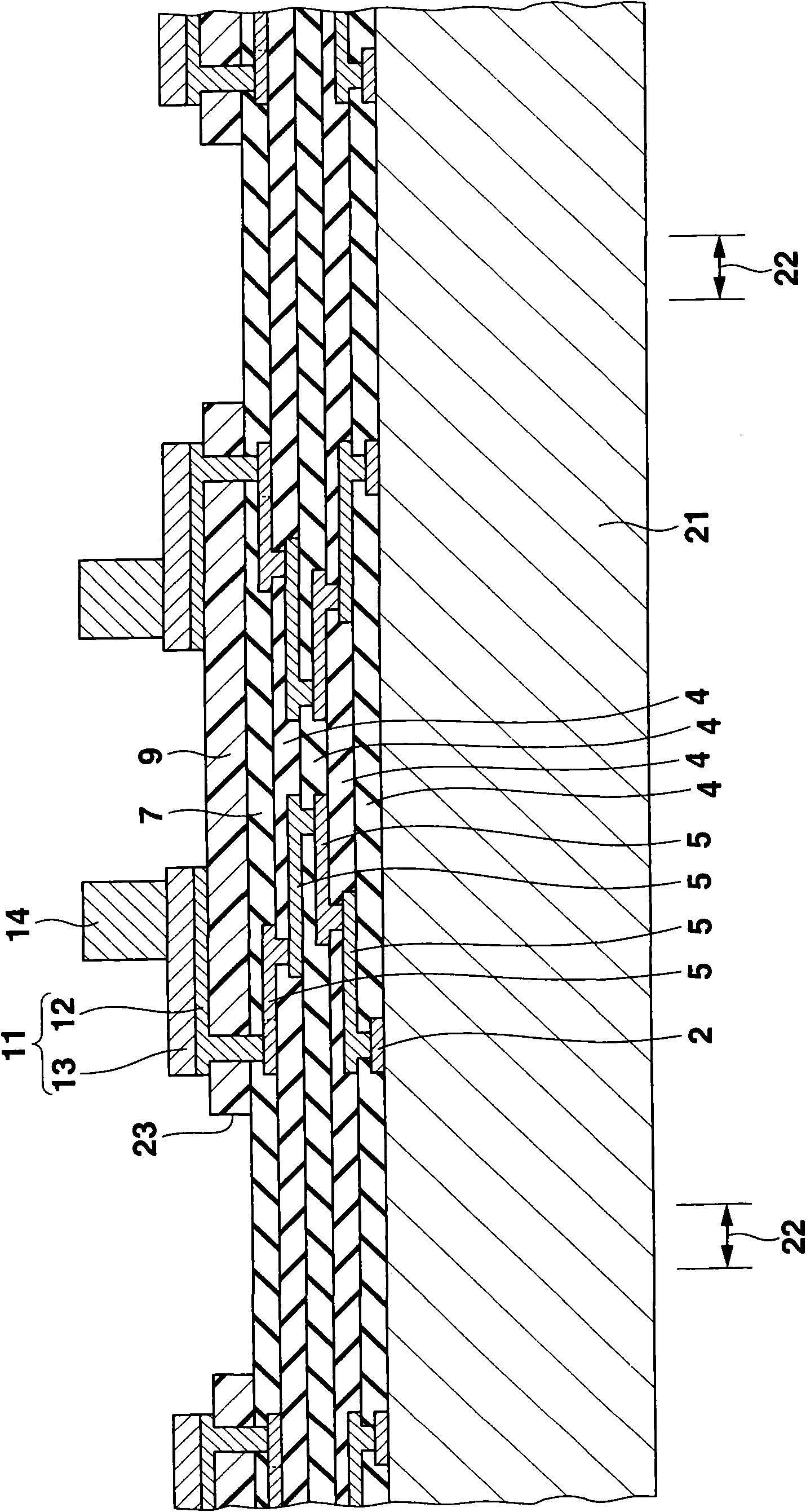
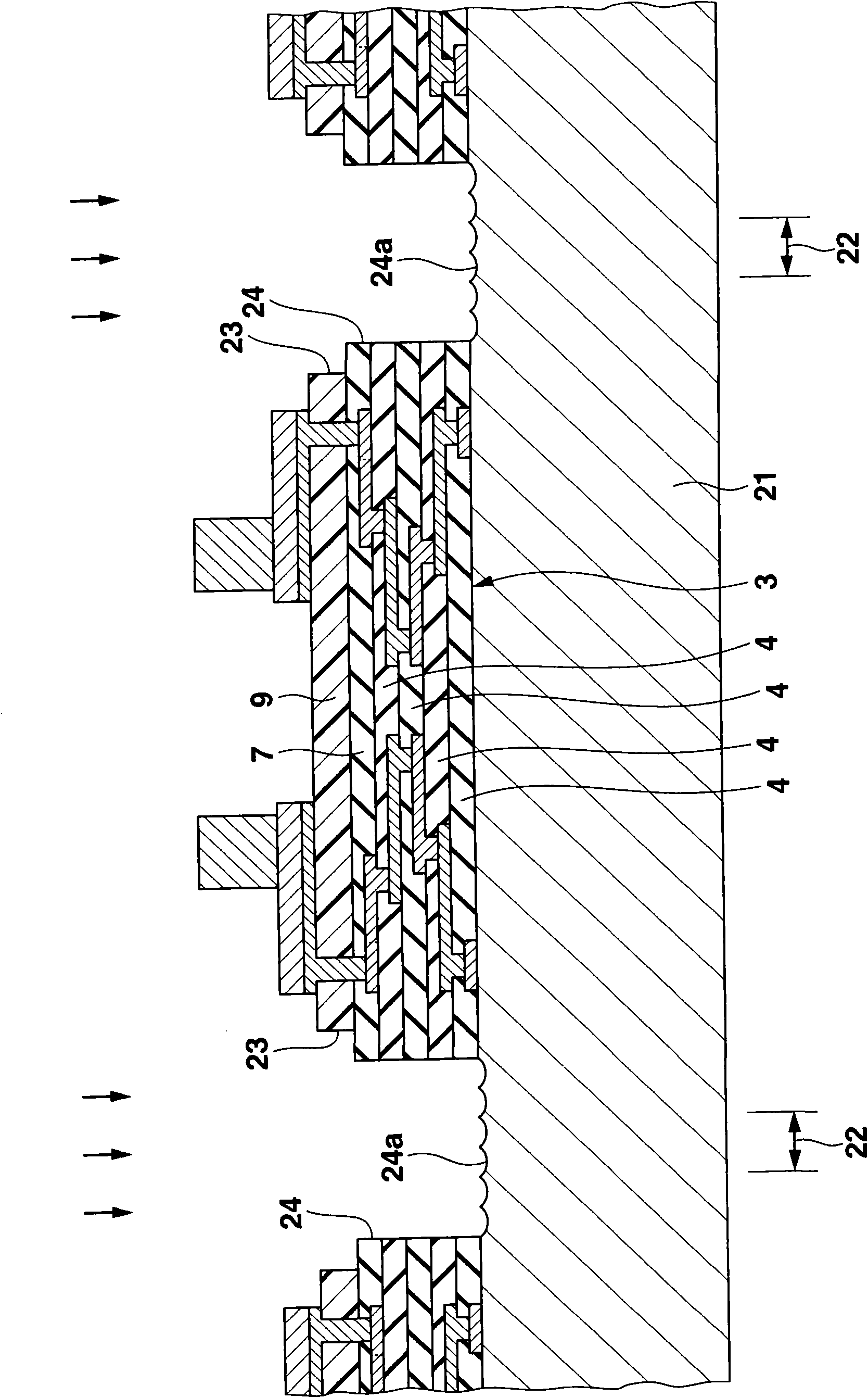
[0059] figure 1 A cross-sectional view showing a semiconductor device according to a first embodiment of the present invention. This semiconductor device includes a silicon substrate (semiconductor substrate) 1 . On the upper surface of the silicon substrate 1, integrated circuits with predetermined functions are provided, especially elements (not shown) such as transistors, diodes, resistors, capacitors, etc. Connection pads 2 made of aluminum-based metal or the like. Although only two connection pads 2 are shown in the figure, there are actually a plurality of connection pads 2 on the upper surface of the silicon substrate.

[0060] On the upper surface of the silicon substrate 2 except for the outer peripheral portion of the connection pad 2, a low dielectric constant film wiring multilayer structure portion 3 for connecting the various elements of the above-mentioned integrated circuit is provided. The low-dielectric-constant film wiring laminated structure portion 3 ha...

no. 2 approach

[0086] Figure 13 It is a cross-sectional view of a semiconductor device as a second embodiment of the present invention. In this semiconductor device, with figure 1 The semiconductor device shown differs in having the second trench 26 with a depth ratio Figure 4 The case shown is a shallow construction. Therefore, in the lower portion of the peripheral side surface of the silicon substrate 1, between the lower surface of the silicon substrate 1 and the second groove 26, a remaining portion of the silicon substrate 1 is formed as a protrusion 31 whose side surface is exposed (exposed) to the outside. The side surface of the protruding portion 31 exposed to the outside is flush with the side surface of the sealing film 15 . In this way, the lower protective film 18 formed on the lower surface of the silicon substrate 1 covers the lower surface of the protrusion 31 .

[0087] Next, an example of a method of manufacturing the semiconductor device will be described. At this ...

no. 3 approach

[0094] Figure 18 It is a cross-sectional view of a semiconductor device as a third embodiment of the present invention. In this semiconductor device, with Figure 13 The semiconductor device shown is different in that the protrusion 31 is removed by forming the third groove 32 in the shape of a track until the sealing film 15 is exposed on the peripheral portion of the lower surface of the silicon substrate 1 including the protrusion 31, and the third The lower protective film 18 is provided in the groove 32 .

[0095] Next, an example of a method of manufacturing the semiconductor device will be described. At this time, at Figure 15 After the procedure shown, as Figure 19 As shown, a cutting knife 33 is prepared. The cutting blade 33 is made of a disc-shaped whetstone, the cross-sectional shape of the cutting edge is substantially U-shaped, and the thickness is larger than the width of the second groove 26 . Then, using the cutting knife 33, will include the second g...


PUM


Abstract

The invention provides a semiconductor device and a manufacturing method thereof; wherein, a stacked structure part of a low dielectric constant film and wiring formed by the low dielectric constant film (4) and wiring (5) is arranged on the region on the upper surface of a silicon substrate (1) except the periphery; a sealing film (15) is used for covering the periphery side of the stacked structure part (3) of the low dielectric constant film and wiring. Therefore, the structure that the low dielectric constant film (4) can not easily be stripped is formed. To protect the lower surface fromcracking, a lower layer of protective film (18) is arranged at the lower surface of the silicon substrate (1).

Description

technical field [0001] The present invention relates to a semiconductor device having a low dielectric constant film and a method of manufacturing the same. Background technique [0002] A CSP (Chip Size Package) having substantially the same size (dimensions and dimensions) as a semiconductor substrate is known as a semiconductor device mounted in a small electronic device represented by a portable electronic device. Among CSPs, a package that is packaged in a wafer state and separated into individual semiconductor devices by dicing is also called WLP (Wafer Level Package). [0003] Japanese Patent Application Laid-Open No. 2004-349461 discloses a semiconductor device in which wiring is extended on the upper surface of an insulating film covering connection pads formed on a semiconductor substrate, and the extended wiring is A plurality of columnar electrodes are provided on the upper surface of the connection pad portion formed at one end, and a sealing film is formed to ...

Claims


Application Information

Patent Timeline
Patent Type & Authority Applications(China)
IPC IPC(8): H01L23/485H01L23/28H01L21/768
CPCH01L2924/01019H01L24/96H01L2224/13H01L2924/14H01L2224/94H01L2224/12105H01L2224/04105H01L2924/3512H01L2924/00H01L2224/03
Inventor 小六泰辅若林猛冈田修桑原治盐田纯司藤井信充
Owner TERAMIKROS INC
Why Eureka
Try Eureka