Architecture of power supply system for LCD apparatus

Inactive Publication Date: 2005-10-27
DELTA ELECTRONICS INC
6 Cites 38 Cited by

AI-Extracted Technical Summary

Problems solved by technology

The relatively lower efficiencies of the PFC circuits with the power frequency rectifiers and the hot spots caused by their components in the above-mentioned technologies of the prior art are the problems relatively hard to overcome especially for the application occasions having the higher power.
Besides, the 3 stage power conversion, including the PFC circuit, the...

Benefits of technology

[0004] It is therefore an object of the present invention to propose a new architecture of a power supply system for offering a backlight power of an apparatus. A Dual Boost PFC circuit is employed to convert the input AC voltage to a DC bus voltage and to accomplish the functions of the PFC of the input current, at least one inverter is electrically connected to the proposed Dual Boost PFC circuit for dr...

Abstract

The proposed architecture includes a Dual Boost PFC circuit for receiving the AC input voltage and generating the DC bus voltage, at least one inverter coupled to the Dual Boost PFC circuit for driving at least one CCFL to offer a backlight of a LCD panel, and a DC/DC converter coupled to the Dual Boost PFC circuit for offering power to the LCD apparatus. Since neither the input bridge rectifier nor the DC/DC converter between the PFC circuit and the backlight inverter is included in the presented architecture, relatively the simpler configuration and the higher conversion efficiency than those of the prior art are achieved.

Application Domain

Technology Topic

Image

  • Architecture of power supply system for LCD apparatus
  • Architecture of power supply system for LCD apparatus
  • Architecture of power supply system for LCD apparatus

Examples

  • Experimental program(1)

Example

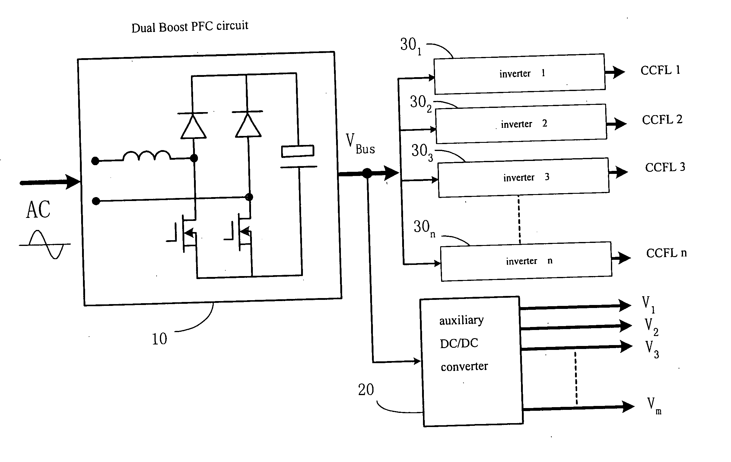
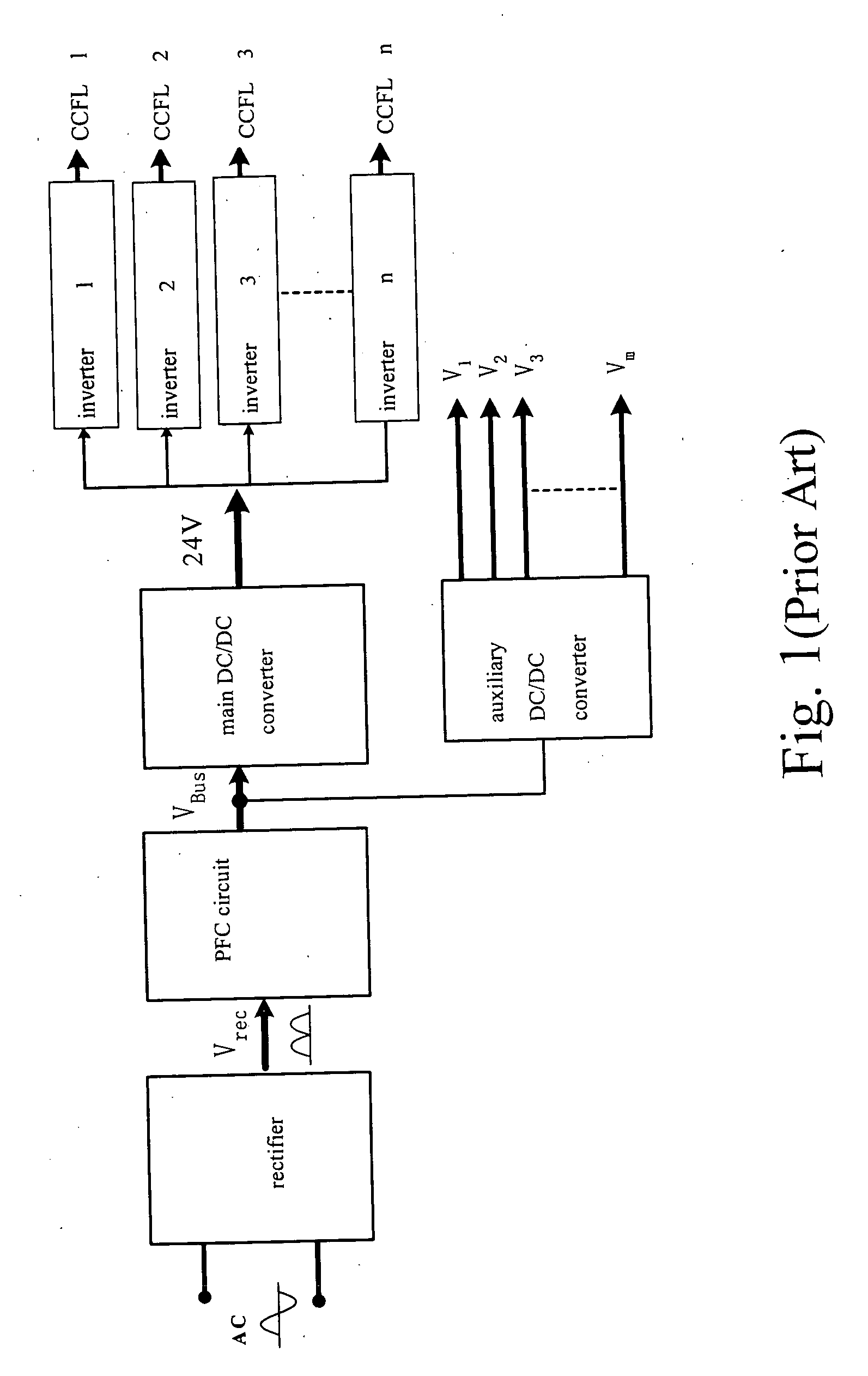
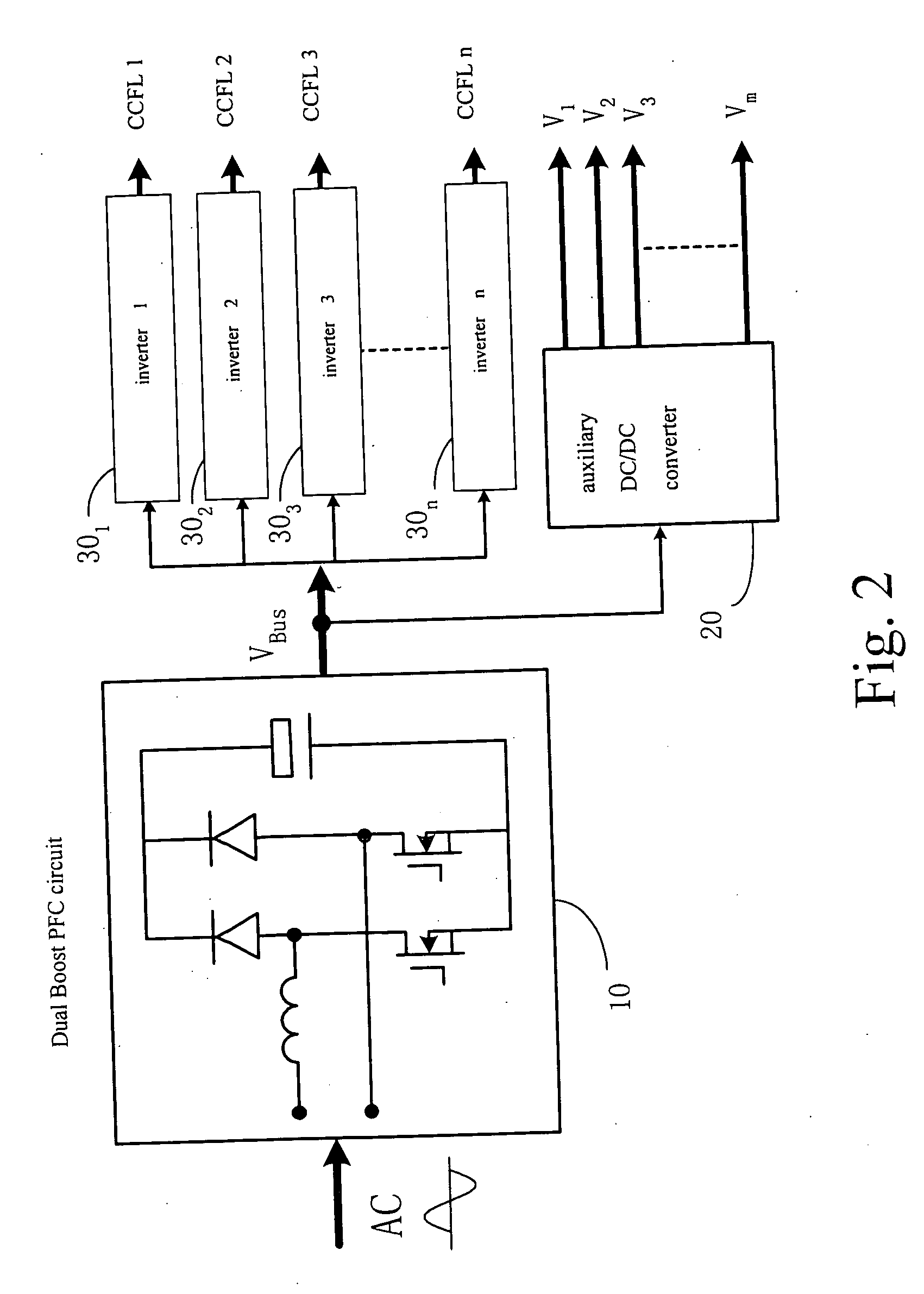
[0025] Please refer to FIG. 2, it shows the schematic circuit diagram of the first preferred embodiment of the power supply system architecture of the LCD apparatus of the present invention. In which, the input terminals of a Dual Boost PFC circuit 10 of the front stage are directly connected to the utility AC power network, the input utility AC voltage is converted to a stable DC bus voltage VBUS. A plurality of inverters, 301, 302, . . . , and 30n, for driving corresponding CCFLs, CCFL1, CCFL2, . . . , and CCFLn, to offer the backlight of the LCD panel. The input terminals of these inverters, 301, 302, . . . , and 30n, are electrically connected to the output terminals of the Dual Boost PFC circuit 10, and the input voltage for each of these inverters, 301, 302, . . . , and 30n, is the output voltage of the Dual Boost PFC circuit 10, VBUS. The input terminals of a DC/DC converter 20 are also electrically connected to the output terminals of the Dual Boost PFC circuit 10 for generating a plurality of output voltages, V1, V2, . . . , and Vm, desired by the control components of the LCD apparatus. Since the rectifier at the input side and the DC/DC converter between the PFC circuit and the backlight inverter of the conventional architecture as shown in FIG. 1 are both omitted in the proposed new architecture, the power consumptions of the LCD apparatus of the present invention are less than those of the conventional architecture, and the conversion efficiency of the proposed architecture is relatively higher, which is more suitable for the self-cooling working conditions. Meanwhile, relatively the simpler configuration and the lower manufacturing costs are also achieved by the proposed architecture.
[0026] Please refer to FIG. 3, it shows the equivalent circuit diagram of the first preferred embodiment of the Dual Boost PFC circuit of the power supply system architecture of the LCD apparatus of the present invention. In which, the first diode D1 and the first power switch Q1 (a MOSFET) is electrically connected in series at the first connecting node, the second diode D2 and the second power switch Q2 (also a MOSFET) is electrically connected in series at the second connecting node, and these two series-connected combinations constitute two bridge legs electrically connected in parallel. The cathode of the first diode D1 included in the first upper leg and the cathode of the second diode D2 included in the second upper leg are electrically connected, and are electrically connected to the first terminal (the anode) of the output capacitor CB. The source of the first switch Q1 included in the first lower leg and the source of the second switch Q2 included in the second lower leg are electrically connected, and are electrically connected to the second terminal (the cathode) of the output capacitor CB. The AC input voltage having low frequency, vac, is electrically connected to a boost inductor L in series, and the series-connected combination of the boost inductor and the AC input voltage, vac, is electrically connected across the first and the second connecting nodes of the first and the second bridgelegs respectively.
[0027] Please refer to FIG. 4, it shows the operational principles of the equivalent circuit diagram of the Dual Boost PFC circuit as shown in FIG. 3. According to the reference directions of the variables defined in FIG. 3, the boost inductor L, the first switch Q1, the first diode D1, and the output capacitor CB constitute a basic boost PFC circuit in the positive half cycle of the input voltage vac, the second switch Q2 is kept in the turned on status, and the current flows through the second switch Q2 having the same amount of current that flows through the boost inductor L but in the reverse direction. The boost inductor L, the second switch Q2, the second diode D2, and the output capacitor CB constitute a basic boost PFC circuit in the negative half cycle of the input voltage vac, the first switch Q1 is kept in the turned on status, and the current flows through the first switch Q1 having the same amount of current that flows through the boost inductor L but in the reverse direction. This circuit could be employed to fulfill the PFC functions by two boost PFC circuits at the positive and the negative half cycles respectively, thus a power frequency rectifier is not required.
[0028] Though it shows the case of the Dual Boost PFC circuit operated in DCM boundary as shown in FIG. 4, however, it should be pointed out that the control methods of which in the real applications are not limited to that only.
[0029] Besides, the first and the second switches Q1 and Q2 are not only restricted to the MOSFETs, they could be other power switch elements too.
[0030] Furthermore, the preferred embodiments of the Dual Boost PFC circuit as shown in FIG. 2 are not limited to the accomplishment of FIG. 3. Actually, if there are two diodes and two power switch elements to constitute a bridge structure similar to that of FIG. 3, and assuming that certain control method is employed, the AC/DC conversion and the PFC functions could be accomplished simultaneously.
[0031]FIG. 5 is the schematic circuit diagram of the second preferred embodiment of the present invention. In which, the two power switch elements of the Dual Boost PFC circuit 10 constitute the two upper legs of the two bridge legs electrically connected in parallel, and the two diodes constitute the second lower bridge leg.
[0032]FIG. 6 is the schematic circuit diagram of the third preferred embodiment of the present invention. In which, the two power switch elements of the Dual Boost PFC circuit 10 constitute the first bridge leg of the two bridge legs electrically connected in parallel, and the two diodes constitute the second bridge leg.
[0033]FIG. 7 is the schematic circuit diagram of the fourth preferred embodiment of the present invention. In which, the two diodes of the Dual Boost PFC circuit 10 constitute the first bridge leg of the two bridge legs electrically connected in parallel, and the two power switch elements constitute the second bridge leg.
[0034] In conclusion, the architecture of the power supply system disclosed in the present invention, which has neither the input rectifier nor the DC/DC converter between the PFC circuit and the backlight inverters of the prior art disclosed in FIG. 1. Likewise, the proposed circuit does not have any bridge rectifier of the aforementioned circuit for offering the power to CCFL in the prior art, which includes a bridge rectifier, a PFC circuit (or a boost circuit) coupled to the rectifier, and an inverter coupled to the PFC circuit, and the problem of having relatively lower efficiencies of the PFC circuits in the prior art is solved effectively. Therefore, relatively the simpler configuration and the lower manufacturing costs, the higher conversion efficiency, and the thermal design more suitable for the self-cooling working conditions than those in the prior art could be achieved by the proposed architecture of the present invention.
[0035] While the invention has been described in terms of what are presently considered to be the most practical and preferred embodiments, it is to be understood that the invention need not be limited to the disclosed embodiment. On the contrary, it is intended to cover various modifications and similar arrangements included within the spirit and scope of the appended claims, which are to be accorded with the broadest interpretation so as to encompass all such modifications and similar structures. Therefore, the above description and illustration should not be taken as limiting the scope of the present invention which is defined by the appended claims.

PUM

no PUM

Description & Claims & Application Information

We can also present the details of the Description, Claims and Application information to help users get a comprehensive understanding of the technical details of the patent, such as background art, summary of invention, brief description of drawings, description of embodiments, and other original content. On the other hand, users can also determine the specific scope of protection of the technology through the list of claims; as well as understand the changes in the life cycle of the technology with the presentation of the patent timeline. Login to view more.

Similar technology patents

Light-emitting device and projector

InactiveUS20110303892A1Conversion efficiency be highProjectorsDiodePhysicsSecondary layer
Owner:SEIKO EPSON CORP

Rigidly mounted tracking solar panel and method

InactiveUS20170104444A1Conversion efficiency be highLow material costPhotovoltaic supportsSolar heating energyElectricitySunlight
Owner:THE BOEING CO

Power generating device

InactiveUS20140132100A1Small rotational resistanceConversion efficiency be highMagnetic circuit shape/form/constructionSynchronous machines with stationary armatures and rotating magnetsEngineeringElectrical resistance and conductance
Owner:SHINSEI SHOWJI

Classification and recommendation of technical efficacy words

  • Conversion efficiency be high

Semiconductor device

InactiveUS20100001790A1Reduce parasitic inductanceConversion efficiency be highTransistorConversion constructional detailsCapacitanceEngineering
Owner:RENESAS ELECTRONICS CORP

Hamr head spot-size converters with secondary index confinement

ActiveUS20150179197A1Conversion efficiency be highCombination recordingArm with optical waveguideEngineeringLaser diode
Owner:WESTERN DIGITAL TECH INC
Why Eureka
Try Eureka