Programmable system on a chip

a programmable logic and chip technology, applied in the field of integrated circuit devices, can solve the problems of fpgas and other programmable logic devices (plds) being limited to providing digital logic functions that are programmabl

Active Publication Date: 2005-10-27
MICROSEMI SOC
View PDF69 Cites 109 Cited by
  • Summary
  • Abstract
  • Description
  • Claims
  • Application Information

AI Technical Summary

Problems solved by technology

Traditionally, FPGAs and other programmable logic devices (PLDs) have b

Method used


Image

  • Programmable system on a chip
  • Programmable system on a chip
  • Programmable system on a chip

Examples


Embodiment Construction

[0029] Those of ordinary skill in the art will realize that the following description of the present invention is illustrative only and not in any way limiting. Other embodiments of the invention will readily suggest themselves to such skilled persons.

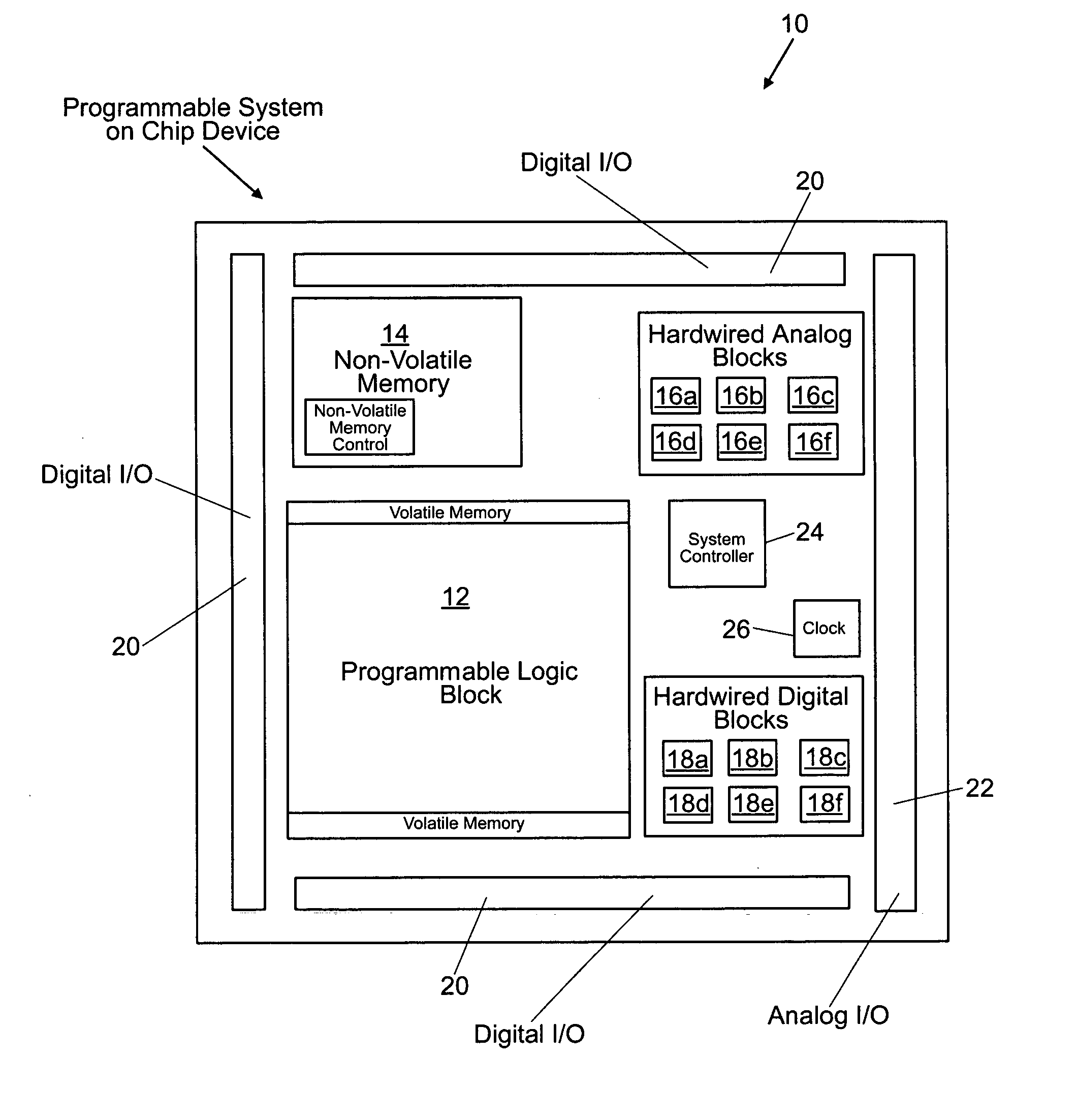
[0030] The term “system-on-a-chip” or “SOC” generally refers to an integrated circuit device that includes multiple types of integrated circuits on a single die, where the circuits are of types that have traditionally been constructed on separate silicon wafers.

[0031] An SOC 10 according to the present invention design is shown generally in a block-diagram architectural level drawing in FIG. 1, which shows its main components. As shown in FIG. 1, an illustrative embodiment of the present invention is a system-on-a-chip integrated circuit 10 that includes a programmable logic block 12, at least one non-volatile memory block 14, analog ASIC circuit blocks 16a through 16f, digital ASIC circuit blocks 18a through 18f, digital input / outpu...


PUM


Abstract

A programmable system-on-a-chip integrated circuit device comprises a programmable logic block, a non-volatile memory block, an analog sub-system, an analog input/output circuit block, and a digital input/output circuit block. A programmable interconnect architecture includes programmable elements and interconnect conductors. Ones of the programmable elements are coupled to the programmable logic block, the non-volatile memory block, the analog sub-system, the analog input/output circuit block, the digital input/output circuit block, and to the interconnect conductors, such that inputs and outputs of the programmable logic block, the non-volatile memory block, the analog sub-system, the analog input/output circuit block, and the digital input/output circuit block can be programmably coupled to one another.

Description

CLAIM FOR PRIORITY [0001] This application claims priority from U.S. Provisional Patent application Ser. No. 60 / 491,788, filed Jul. 31, 2003.BACKGROUND OF THE INVENTION [0002] 1. Field of the Invention [0003] The present invention relates to integrated circuits. More particularly, the present invention relates to a system-on-a-chip integrated circuit device including a programmable logic block, at least one user non-volatile memory block, and analog circuits on a single semiconductor integrated circuit chip, flip chip, face-to-face, or other multiple die configuration. [0004] 2. Background [0005] Field-programmable gate array (FPGA) integrated circuits are known in the art. An FPGA comprises any number of logic modules, an interconnect-routing architecture and programmable elements that may be programmed to selectively interconnect the logic modules to one another and to define the functions of the logic modules. To implement a particular circuit function, the circuit is mapped into...

Claims


Application Information

Patent Timeline
IPC IPC(8): H01LH03K19/177
CPCG01K7/015G06F1/08G06F1/28G06F1/30G06F15/7842G06F15/7867H03K19/1776H03F2203/45136H03F2203/45166H03K17/223H03K19/177H03K19/17732H03F3/45475
Inventor BAKKER, GREGEL-AYAT, KHALEDSPEERS, THEODOREZHU, LIMINSCHUBERT, BRIANBALASUBRAMANIAN, RABINDRANATHKOLKIND, KURTBARRAZA, THOMASNARAYANAN, VENKATESHMCCOLLUM, JOHNPLANTS, WILLIAM
Owner MICROSEMI SOC
Why Eureka
Try Eureka