Wafer cell for immersion lithography

a lithography and wafer cell technology, applied in the field of lithography, can solve the problems of air as the transmitting medium presenting a clear limit to the na and consequently the minimum scaling size, and unable to meet the requirements of lithography, and achieve the effects of reducing the number of wafer cells, and improving the quality of wafer cells

Inactive Publication Date: 2005-10-27
GOOGLE LLC
View PDF2 Cites 354 Cited by
  • Summary
  • Abstract
  • Description
  • Claims
  • Application Information

AI Technical Summary

Problems solved by technology

However, having an index of refraction n=1, air as the transmitting medium presents a clear limit to the NA and consequently to the minimum scaling size.
While the foregoing techniques represent progress in the development of this new technology, a number of practical implementation issues remain, including maintaining a pure, non-obstructing transmission medium and compatibility of the tools and wafer with the liquid medium.
However, problems remain relating to the tendency to form bubbles during the scanning processing.
A water medium is susceptible to forming micro bubbles and nano bubbles in the cavitation prone water layer near the moving surfaces, resulting in imaging obstruction and anomalies.
In addition to problems associated with maintaining purity of the liquid, prior art immersion lithography techniques require substantial redesign of stages for compatibility in a submerged liquid environment requiring significant re-engineering and adding to development costs.
Included among the many issues posed by conventional immersion lithography are modifications to lens design and lens casing for compatibility with the resist and immersion liquid, and maintaining immersion liquid properties such as purity, temperature, etc.

Method used


Image

  • Wafer cell for immersion lithography
  • Wafer cell for immersion lithography
  • Wafer cell for immersion lithography

Examples


Embodiment Construction

[0020] The invention will now be described in more detail by way of example with reference to the embodiments shown in the accompanying figures. It should be kept in mind that the following described embodiments are only presented by way of example and should not be construed as limiting the inventive concept to any particular physical configuration.

[0021] Further, if used and unless otherwise stated, the terms “upper,”“lower,”“front,”“back,”“over,”“under,” and similar such terms are not to be construed as limiting the invention to a particular orientation. Instead, these terms are used only on a relative basis.

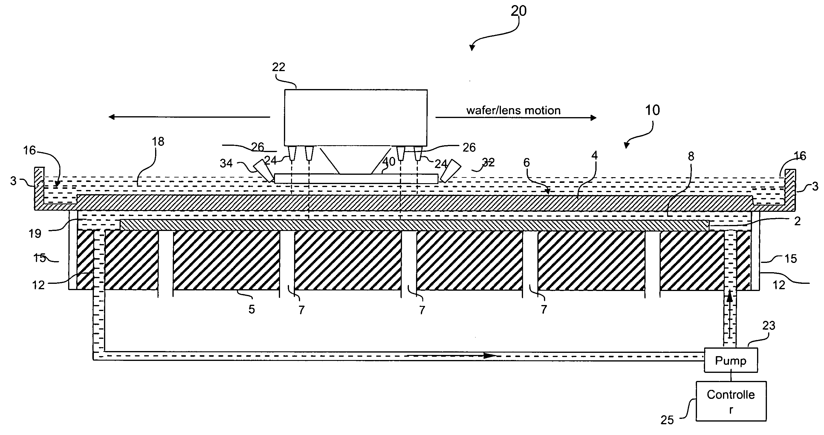
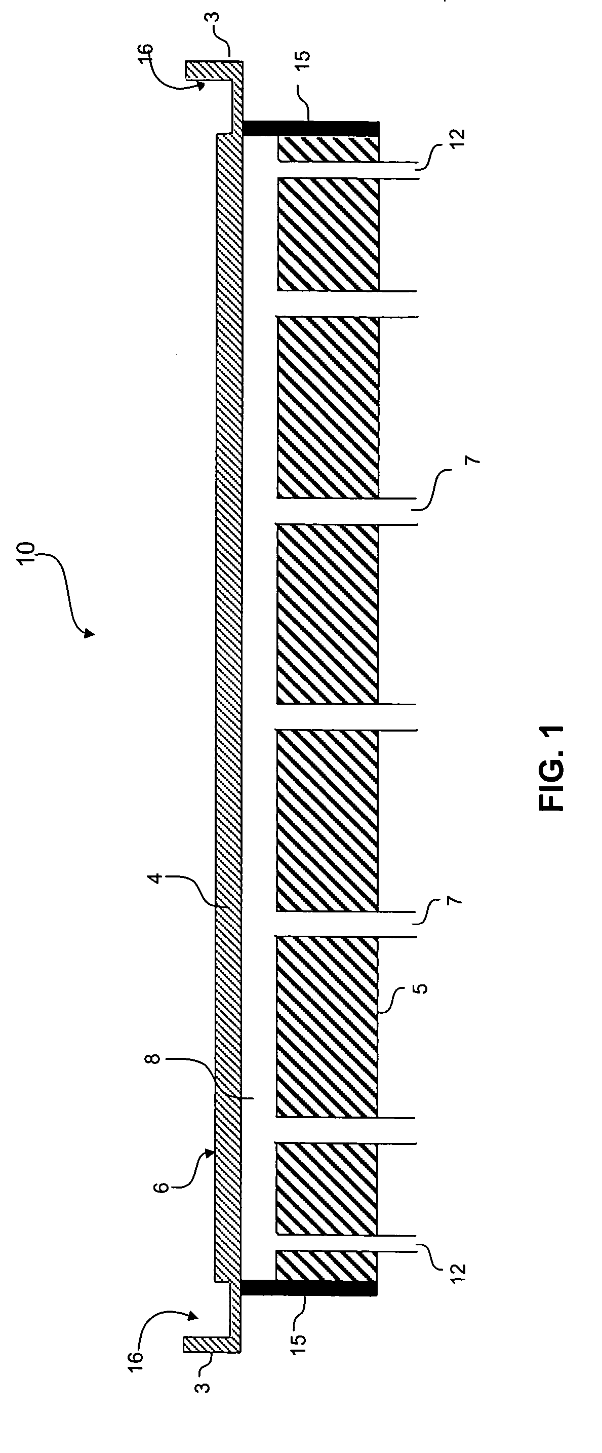
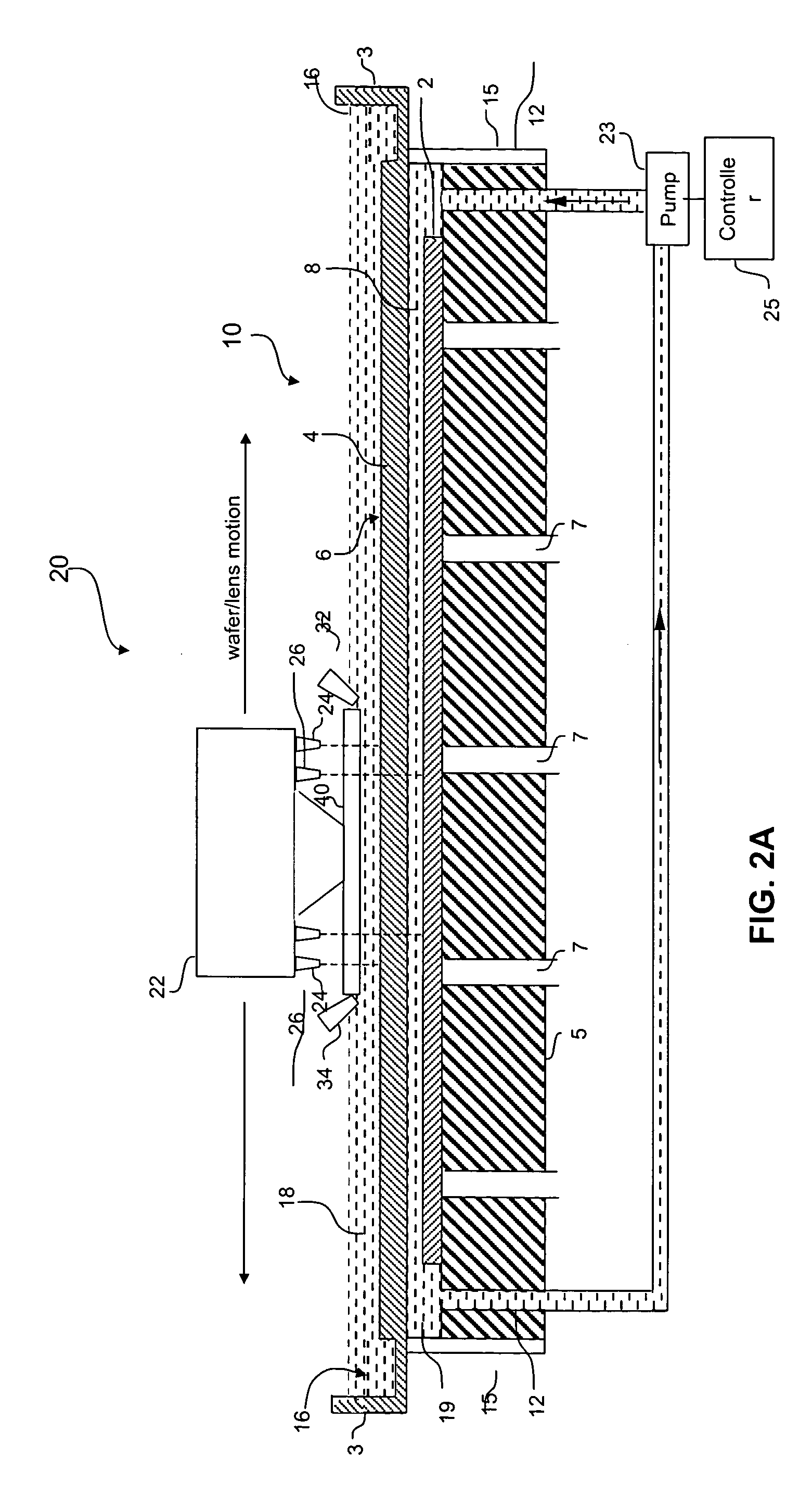
[0022] The present invention is directed toward an improved optical or photolithographic apparatus, system and method in which one or more immersion fluids are utilized to increase the index of refraction and consequently increase the numerical aperture. In one embodiment, the invention employs a layered liquid immersion technique that enables a semiconductor workpiece to b...


PUM

PropertyMeasurementUnit
wavelengthsaaaaaaaaaa
transparentaaaaaaaaaa

Abstract

An apparatus, system and method for use with a photolithographic system. In accordance with one embodiment, the photolithographic system of the present invention includes a workpiece support member for supporting a semiconductor wafer. A substantially transparent cover member is disposed over the workpiece support member to form a substantially enclosed workpiece cell therebetween. The enclosed workpiece cell is filled with a first immersion fluid having suitable refractive properties. The cover member, having suitable refractive properties, includes an upper surface contoured to form an open reservoir containing a second immersion fluid, having suitable refractive properties, and in which a final lens element may be immersed during a lithography process.

Description

BACKGROUND OF THE INVENTION [0001] 1. Field of the Invention [0002] The present invention generally relates to lithography for semiconductor fabrication, and in particular, to utilizing a liquid medium through which a semiconductor substrate is illuminated during optical lithography. More particularly, the present invention relates to an immersion lithography method and apparatus that employs a contained wafer immersion cell to increase the numerical aperture while minimizing sources of photolithographic light obstruction. [0003] 2. Background Information [0004] Lithography, in the context of building integrated circuits (ICs) such as microprocessors and memory chips, is a highly specialized printing process used to put detailed patterns onto silicon wafers. An image containing the desired pattern is projected onto the wafer through a mask defining the pattern. Prior to light projection through the mask, the wafer is coated with a thin layer of photosensitive etch resistant material...

Claims


Application Information

Patent Timeline
Patent Type & Authority Applications(United States)
IPC IPC(8): G03B27/52G03F7/20
CPCG03F7/70341
Inventor FURUKAWA, TOSHIHARUHAKEY, MARK CHARLESHORAL, DAVID VACLAVKOBURGER, CHARLES WILLIAM IIIMITCHELL, PETER H.
Owner GOOGLE LLC
Why Eureka
Try Eureka