Method and apparatus for removing and/or preventing surface contamination of a probe

Inactive Publication Date: 2005-11-03
SOLID STATE MEASUREMENTS
View PDF6 Cites 6 Cited by
  • Summary
  • Abstract
  • Description
  • Claims
  • Application Information

AI Technical Summary

Benefits of technology

[0006] It is an object of the present invention to provide a method and apparatus for removing and/or preventing surface contamination of a probe that overcomes the deficiencies of the prior art. It is another object of the present invention to provide a method and apparatus for removing and/or preventing surface conta

Problems solved by technology

One drawback to using an EM-gate probe is that a surface of the probe that contacts the semiconductor wafer may become contaminated.
Such surface contamination is undesirable, since it adv

Method used


Image

  • Method and apparatus for removing and/or preventing surface contamination of a probe
  • Method and apparatus for removing and/or preventing surface contamination of a probe
  • Method and apparatus for removing and/or preventing surface contamination of a probe

Examples


example

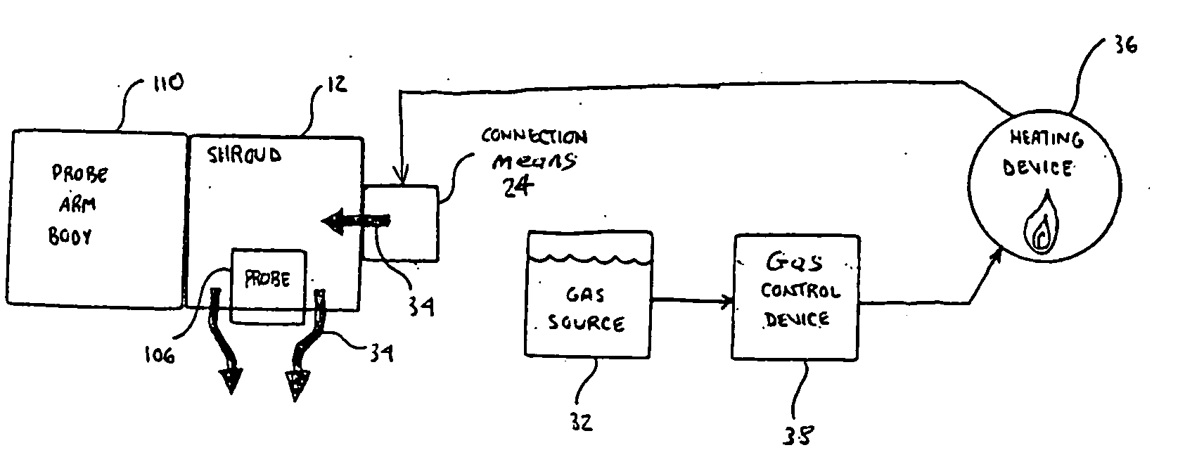
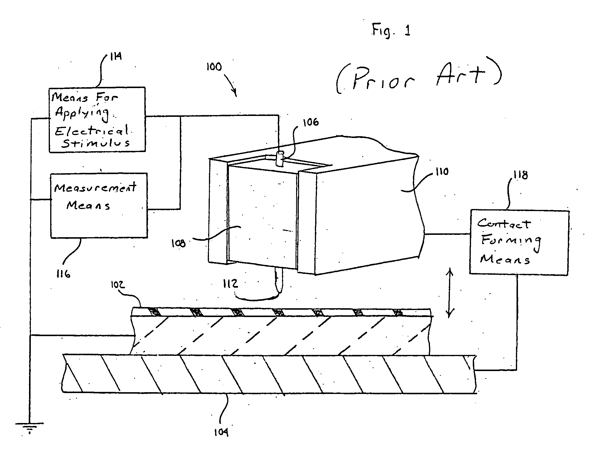
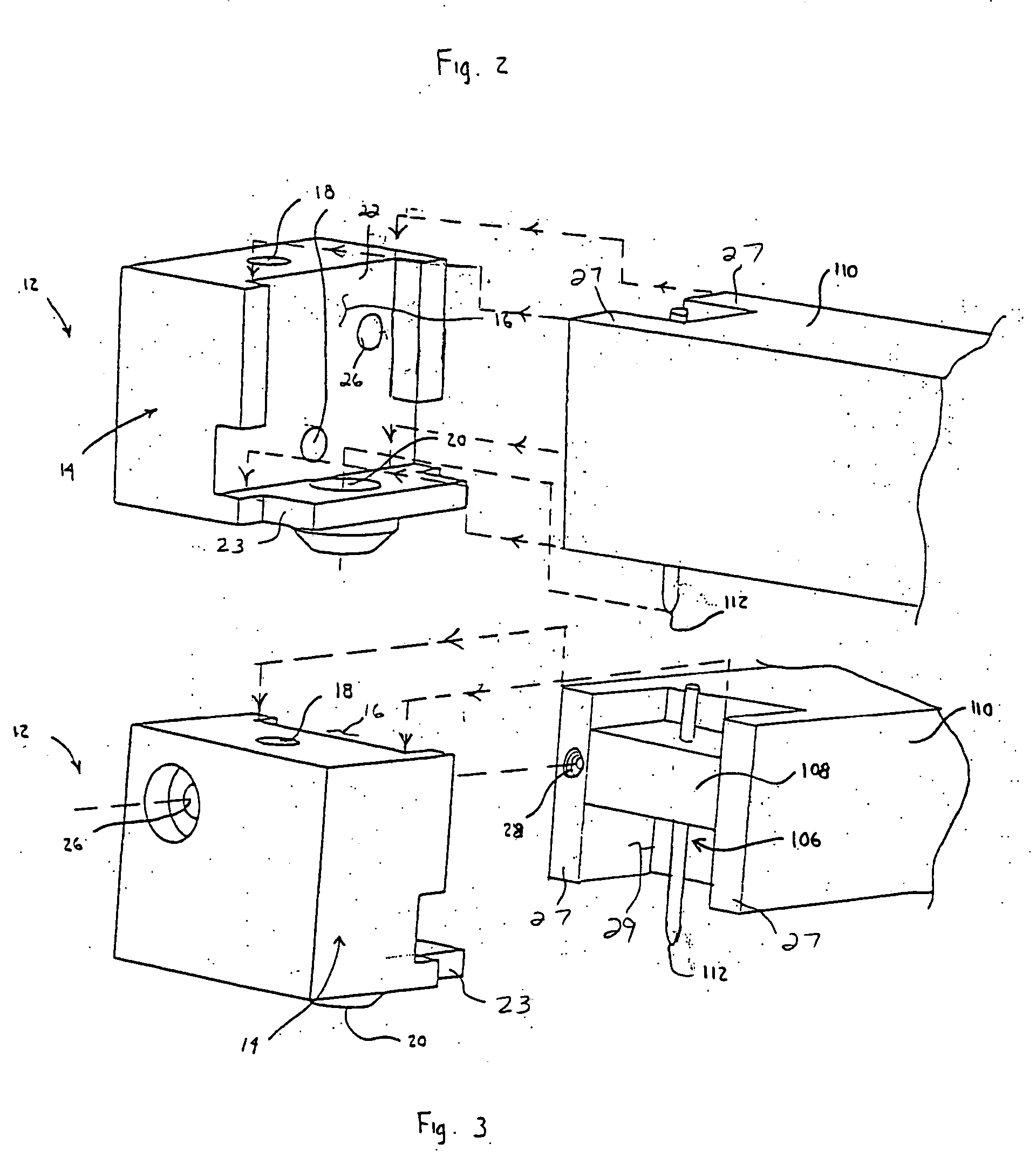
[0029] In one example of the present invention, gas 34 in the form of a heated nitrogen gas is introduced into chamber 30 via inlet passage 18. Contamination removal and / or prevention occurs, in this example, by two independent means working simultaneously. First, contamination removal is achieved through the heating of probe 106, with heating occurring primarily through the mode of forced convection, which occurs as the heated nitrogen gas flows over the surface of probe 106. The second means of contamination removal and prevention is achieved by creating a localized environment that substantially lowers the levels of humidity and other contaminating vapors. In this example, this is achieved through the use of highly purified nitrogen gas, preferably over 99% pure, which displaces the ambient atmosphere around the distal end 112 of probe 106. Since the nitrogen gas is obtained from the liquid or gas nitrogen vessel or from a nitrogen generator, this nitrogen contains almost no wate...


PUM


Abstract

To remove and/or prevent contamination of a probe, at least a portion of the probe is positioned in a chamber having an inlet passage and an outlet passage, with a distal end of the probe extending through the outlet passage and terminating on a side thereof opposite the chamber. A gas is caused to flow through the inlet passage into the chamber and out the outlet passage, thereby modifying an environment surrounding the distal end of the probe. The gas may be heated prior to injection.

Description

BACKGROUND OF THE INVENTION [0001] 1. Field of the Invention [0002] The present invention relates generally to semiconductor wafer probes and, in particular, to a method and apparatus for removing and / or preventing contamination of a surface of the probe, typically around a working or distal end. [0003] 2. Description of Related Art [0004] In the field of semiconductor manufacture, a semiconductor wafer must be tested to determine one or more of its electrical properties prior to or after the formation of integrated circuits thereon. An elastic metal gate (EM-gate) probe may be used to determine these electrical properties. Such a probe desirably includes an elastically deformable conductive tip for contacting a front surface of the semiconductor wafer. An electrical stimulus is applied between the elastically deformable conductive tip and the semiconductor wafer and a response is measured to the electrical stimulus. At least one electrical property of the dielectric and / or the semi...

Claims


Application Information

Patent Timeline
IPC IPC(8): G01R31/26B08B5/00F26B7/00F26B25/00G01Q10/00G01Q60/10G01Q60/14G01Q70/02G01Q70/06G01R1/06G01R3/00G01R31/28H01L21/66
CPCB08B5/00B82Y35/00G01Q60/16G01Q70/02G01R3/00G01Q60/14
Inventor HOWLAND, WILLIAM H. JR.HEALY, JAMES E. JR.
Owner SOLID STATE MEASUREMENTS
Why Eureka
Try Eureka