Semiconductor processing-purpose substrate detecting method and device, and substrate transfer system

a technology of substrate transfer and semiconductors, applied in the direction of material analysis, transportation and packaging, instruments, etc., can solve the problems of difficult to pick up the substrate, inability to determine the position of the substrate with high accuracy, and inability to detect the exact position of the substrate in forward/backward direction, so as to reduce the time for detection and reduce the misalignment

Active Publication Date: 2005-11-03
TOKYO ELECTRON LTD
View PDF6 Cites 19 Cited by
  • Summary
  • Abstract
  • Description
  • Claims
  • Application Information

AI Technical Summary

Benefits of technology

[0023] In any of the first through the fourth point, detection results can be incorporated to the positioning control of the pick (substrate supporting unit) of the transfer robot. By doing this, the pick can be inserted while always making a center of the substrate as a target, so that the substrate can be received on the pick w

Problems solved by technology

Therefore, it is difficult to pick up the substrate while matching the center of the substrate with that of the pick all the time.
Using the conventional substrate detecting device, while it is capable of determining the presence and the protrusion degree with

Method used


Image

  • Semiconductor processing-purpose substrate detecting method and device, and substrate transfer system
  • Semiconductor processing-purpose substrate detecting method and device, and substrate transfer system
  • Semiconductor processing-purpose substrate detecting method and device, and substrate transfer system

Examples


first embodiment

[0036] (First Embodiment)

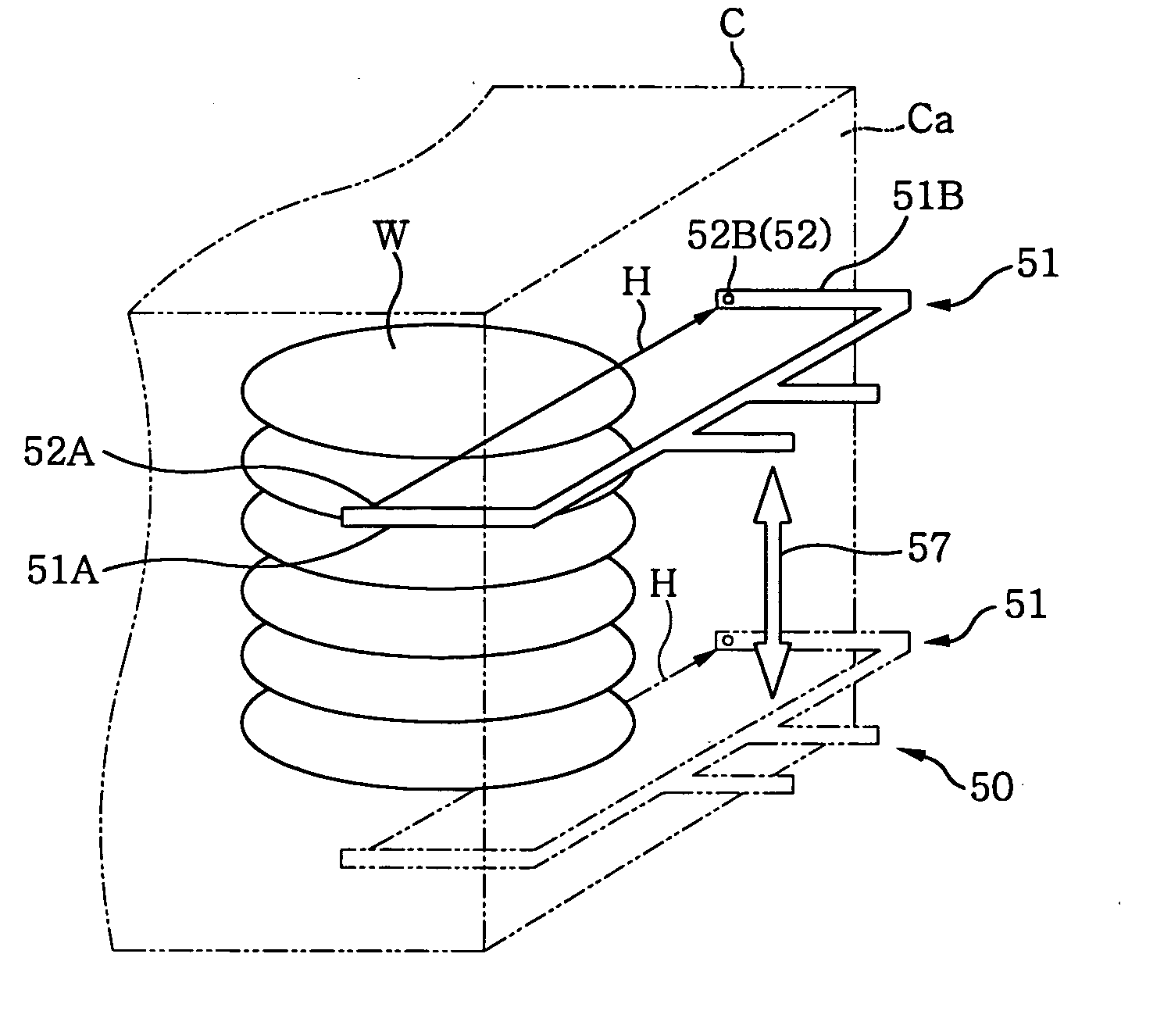
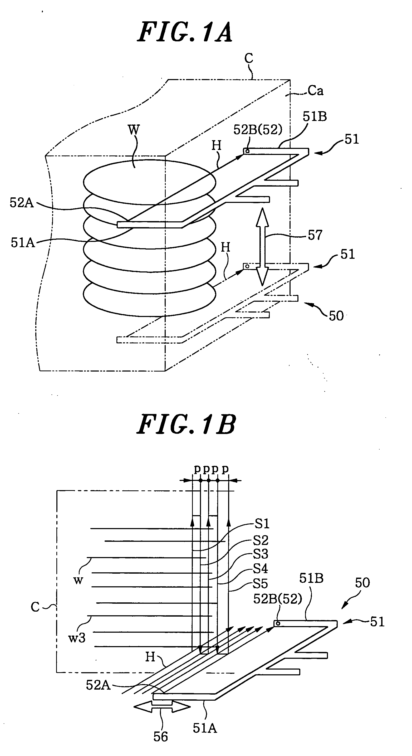
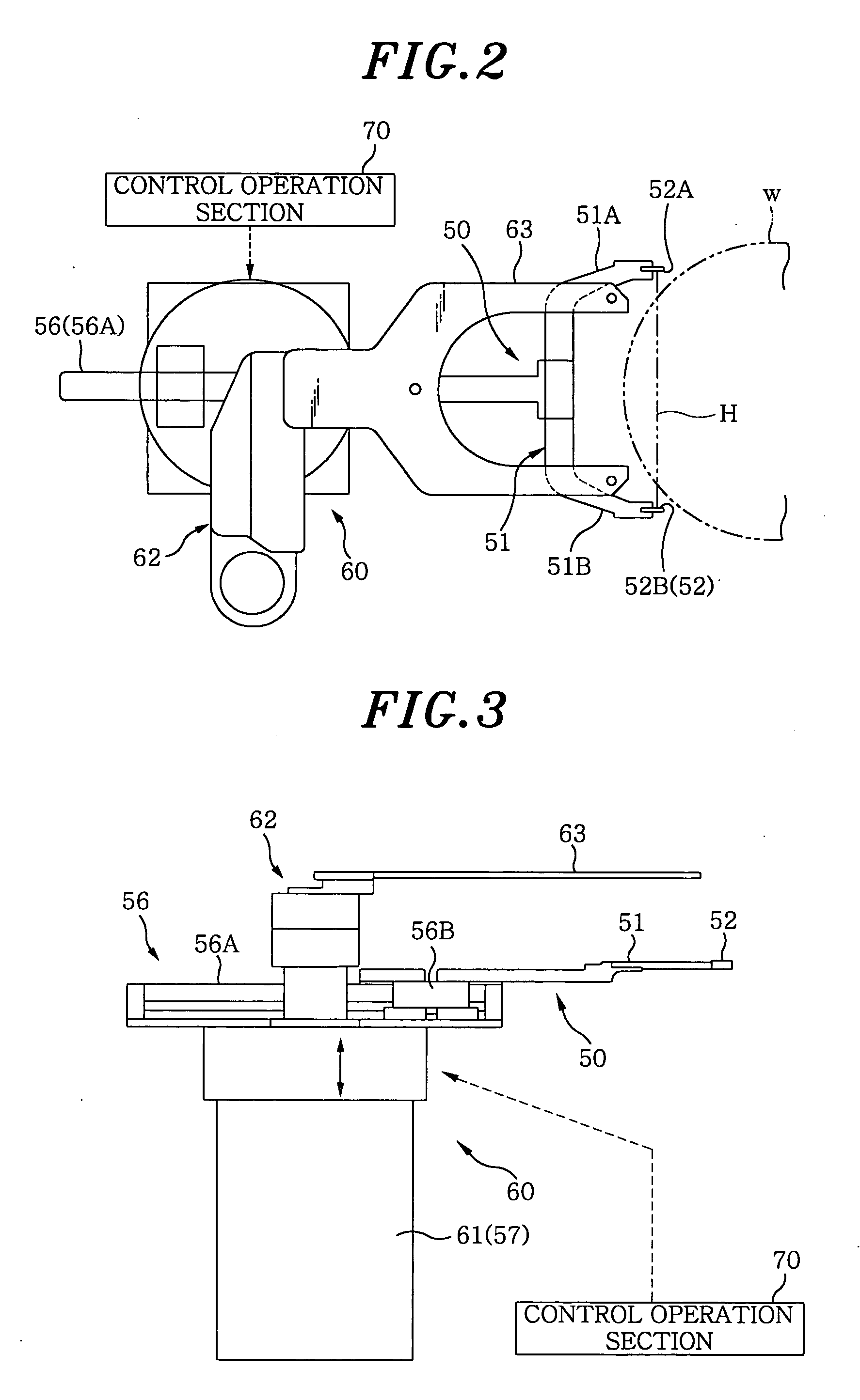
[0037]FIGS. 1A and 1B are of a perspective view and a partial vertical sectional perspective view showing main parts of a substrate detecting device in accordance with a first embodiment of the present invention, respectively. FIG. 2 is a plane view schematically showing a transfer robot for mounting thereon the substrate detecting device in accordance with the first embodiment. FIG. 3 is a side view schematically showing the transfer robot mounting thereon the substrate detecting device described in FIG. 2.

[0038] As shown in FIGS. 2 and 3, a substrate detecting device 50 in accordance with the first embodiment includes a sensor support body 51 mounted on a transfer robot 60. The sensor support body 51 has a pair of arms 51A and 51B separate from and facing each other in a horizontal plane.

[0039] As shown schematically in FIG. 1A, multiple substrates W are accommodated in a cassette C while each being disposed horizontally and having a gap therebetween in ...

second embodiment

[0057] (Second Embodiment)

[0058]FIGS. 4A and 4B are of a perspective view and a partial vertical sectional perspective view showing main parts of a substrate detecting device in accordance with a second embodiment of the present invention, respectively. Further, the substrate detecting device in accordance with the second embodiment is the same as that in the first embodiment, except that a program organization of the control operation section and parts shown in FIGS. 4A and 4B are configured to be different. Namely, the sensor support body 51, the driving sections 56 and 57 thereof, and the transfer robot 60 described in FIGS. 2 and 3 are adopted in the second embodiment as well.

[0059] A substrate detecting device 50B in accordance with the second embodiment includes at least three sets of optical sensors 52 each made up of a light emitting unit 52A and a light receiving unit 52B. Specifically, in the substrate detecting device 50B, five sets of the light emitting units 52A and th...

third embodiment

[0062] (Third Embodiment)

[0063] FIGS. 55A and 5B are of a perspective view and a partial vertical sectional perspective view showing main parts of a substrate detecting device in accordance with a third embodiment of the present invention, respectively. Further, the substrate detecting device in accordance with the third embodiment is the same as that in the first embodiment, except that a program organization of the control operation section and parts shown in FIGS. 5A and 5B are configured to be different. Namely, the sensor support body 51, the driving sections 56 and 57 thereof, and the transfer robot 60 described in FIGS. 2 and 3 are adopted in the third embodiment as well.

[0064] A substrate detecting device 50C in accordance with the third embodiment includes F / L (L is an integer) sets of optical sensors 52 each made up of a light emitting unit 52A and a light receiving unit 52B, for the number of expected total scans F. Specifically, in the substrate detecting device 50C, th...


PUM


Abstract

A detecting device includes a sensor support body having a pair of arms, and an optical sensor having a combination of a light emitting unit and a light receiving unit disposed on one and the other of the arms, respectively. A control operation section controls a driving section and, with the arms inserted in a cassette, the sensor support body is moved, thereby performing a scanning operation for scanning the substrate by the optical sensor. The scanning operation is set such that a light beam is related to the substrate while vertically moving at a plurality of scanning positions. The control operation section finds out the presence of absence of the substrate and the position of the front end of the substrate within the cassette on the basis of data obtained from the optical sensor during scanning.

Description

[0001] This application is a Continuation Application of PCT International Application No. PCT / JP2003 / 16569 filed on Dec. 24, 2003, which designated the United States.FIELD OF THE INVENTION [0002] The present invention relates to a method and apparatus for detecting presence or absence of multiple substrates to be processed and edge location thereof, in semiconductor processing, wherein the multiple substrates are accommodated in a cassette while each being disposed almost horizontally and having a gap therebetween in a vertical direction. Further, the present invention relates to a transfer system for transferring the substrates accommodated in the cassette arranged in the above manner. The term “semiconductor processing” used herein implies various processes to manufacture semiconductor devices and / or a structure including wiring, electrodes, and the like connected to the semiconductor devices on a substrate to be processed, by forming a semiconductor layer, an insulating layer, a...

Claims


Application Information

Patent Timeline
IPC IPC(8): H01L21/00H01L21/68H01L21/67
CPCY10S414/138H01L21/67265H01L21/68
Inventor OKA, HIROKI
Owner TOKYO ELECTRON LTD
Why Eureka
Try Eureka