Method for fabricating flash memory device

a memory device and micro-chip technology, applied in the direction of micro-chip devices, basic electric elements, electrical appliances, etc., can solve the problems of difficult to obtain flash memory devices having a size below sub-micron, difficult to improve the programming and erasing speed of flash memory devices, and the gate does not overlap with the drain region sufficiently to improve, etc., to achieve the effect of improving the efficiency of hot carrier injection

Active Publication Date: 2005-11-03
MARVELL ASIA PTE LTD +1
View PDF8 Cites 28 Cited by
  • Summary
  • Abstract
  • Description
  • Claims
  • Application Information

AI Technical Summary

Benefits of technology

[0027] An object of the present invention is to provide a method for fabricating a flash memory device that improves hot carri

Problems solved by technology

As a result, the gate does not overlap with the drain region sufficiently to improve, optimize or maximize the hot carrier injection efficiency at a low power.
Also, because of certain structural problems, it can be d

Method used


Image

  • Method for fabricating flash memory device
  • Method for fabricating flash memory device
  • Method for fabricating flash memory device

Examples


Embodiment Construction

[0037] Reference will now be made in detail to the preferred embodiments of the present invention, examples of which are illustrated in the accompanying drawings. Wherever possible, the same reference numbers will be used throughout the drawings to refer to the same or like parts.

[0038] Hereinafter, a method for fabricating a flash memory device according to the present invention will be described with reference to the accompanying drawings.

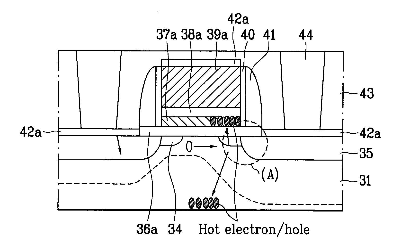
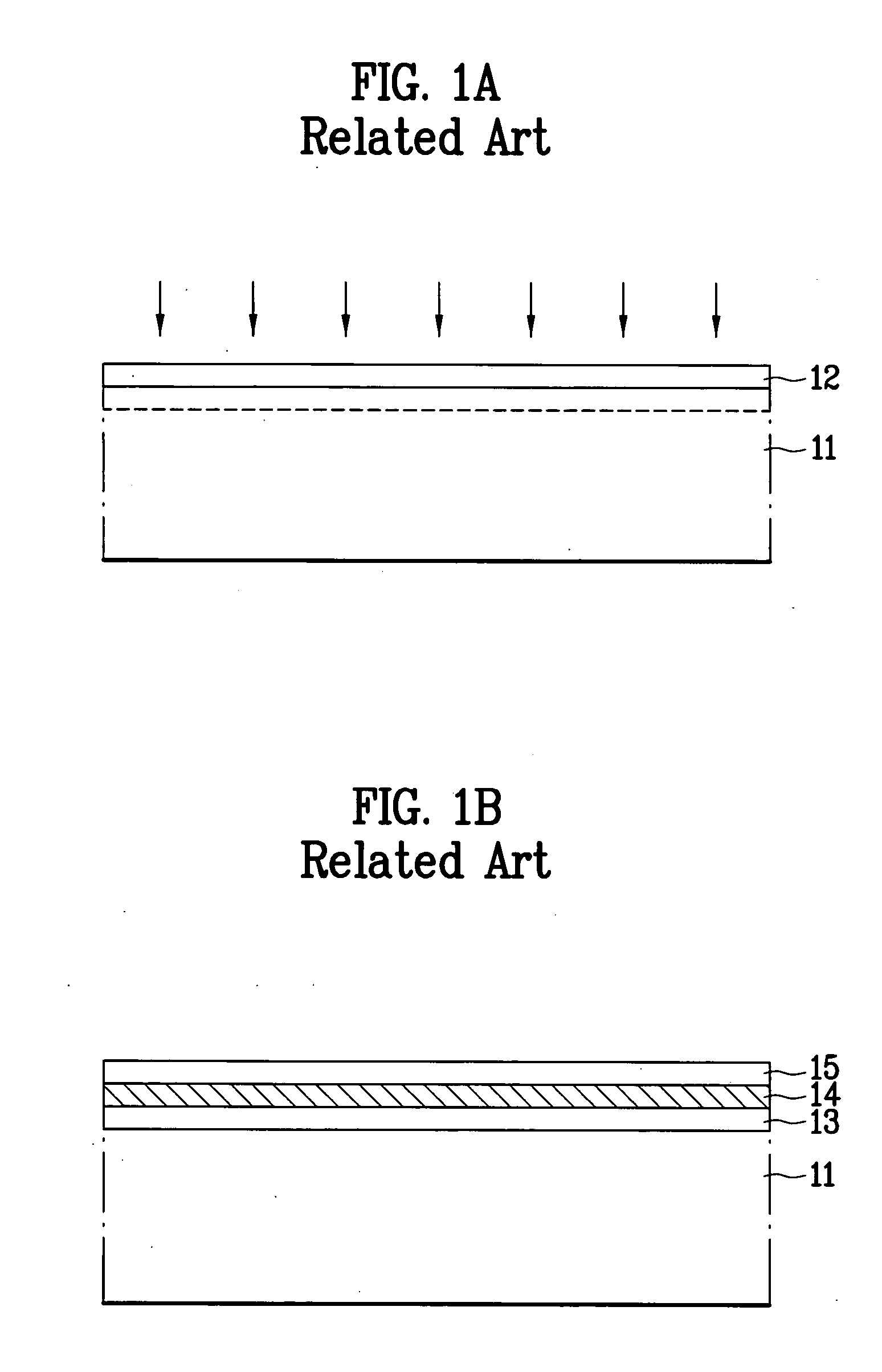
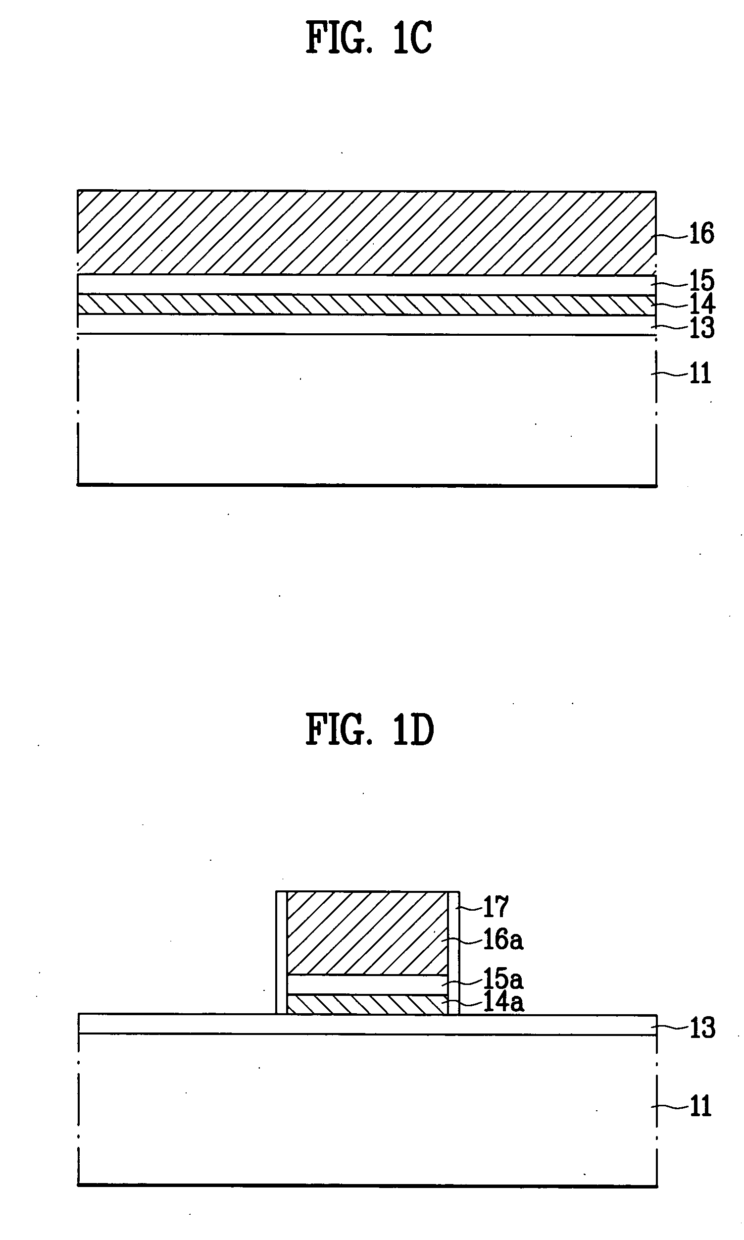
[0039]FIG. 2A to FIG. 2F are cross sectional views of illustrating the process for fabricating an SONOS type flash memory device according to the present invention.

[0040] In a method for fabricating a flash memory device having an SONOS structure according to the present invention, an ion implantation process for forming LDD, source and drain regions is first performed with a sacrificial insulating pattern layer, and then a process for forming a gate dielectric stack structure and a gate is performed, so that it is possible to increase, optimi...


PUM

PropertyMeasurementUnit
Temperatureaaaaaaaaaa
Lengthaaaaaaaaaa

Abstract

A method for fabricating a flash memory device is disclosed that improves hot carrier injection efficiency by forming a gate after forming source and drain implants using a sacrificial insulating layer pattern, which includes forming a sacrificial insulating pattern layer over a flash memory channel region of a semiconductor substrate; forming source and drain regions in the semiconductor substrate by ion implantation using the sacrificial insulating pattern layer as a mask; removing portions of the sacrificial insulating pattern layer; sequentially forming an ONO-type dielectric layer and a gate material layer; selectively etching the gate material layer and at least part of the gate dielectric layer to form a gate; and forming gate sidewall spacers at sides of the gate.

Description

CROSS-REFERENCE TO RELATED APPLICATIONS [0001] This application claims the benefit of Korean Application No. P2004-31011, filed on May 3, 2004, which is hereby incorporated by reference as if fully set forth herein. BACKGROUND OF THE INVENTION [0002] 1. Field of the Invention [0003] The present invention relates to a semiconductor memory device, and more particularly, to a method for fabricating a flash memory device that improves hot carrier injection efficiency by forming a gate after forming source and drain implants using a sacrificial insulating layer pattern. [0004] 2. Discussion of the Related Art [0005] Recently, flash memory devices in common use have been classified into a stacked gate flash cell type and an SONOS (polysilicon-oxide-nitride-oxide-semiconductor) flash cell type. The stacked gate flash cell type has a stack structure including a floating gate and a control gate. The SONOS flash cell type comprises an ONO (oxide-nitride-oxide) gate dielectric and a single gat...

Claims


Application Information

Patent Timeline
IPC IPC(8): H01L27/115H01L21/265H01L21/28H01L21/336H01L29/51H01L29/792
CPCH01L21/26586H01L21/28185H01L21/28282H01L29/792H01L29/518H01L29/66545H01L29/66833H01L29/513Y10S438/926H01L29/40117
Inventor SHIN, EUN JONG
Owner MARVELL ASIA PTE LTD
Why Eureka
Try Eureka