Semiconductor device, and method for manufacturing semiconductor device

a semiconductor and semiconductor technology, applied in semiconductor devices, diodes, electrical devices, etc., can solve the problems of increasing recovery loss, deteriorating recovery characteristics, and often affecting the recovery of fwd, so as to improve energization capacity, increase minority carrier injection efficiency, and prolong carrier life

Pending Publication Date: 2022-07-14
MITSUBISHI ELECTRIC CORP
View PDF0 Cites 0 Cited by
  • Summary
  • Abstract
  • Description
  • Claims
  • Application Information

AI Technical Summary

Benefits of technology

[0025]A first aspect of a technique disclosed in the specification of the present application is a semiconductor device including: an IGBT; and an FWD. The IGBT and the FWD are formed on an identical SiC semiconductor substrate, and the IGBT and the FWD are connected in antiparallel. The IGBT includes: a first drift layer of a first conductivity type, a collector region of a second conductivity type on a lower surface of the first drift layer, a base region of a second conductivity type selectively formed in a surface layer of the first drift layer, an emitter region of a first conductivity type selectively formed in a surface layer of the base region, an insulating film in contact with the base region sandwiched between the emitter region and the first drift layer, a gate electrode in contact with the insulating film, and a first high carrier lifetime region formed at a position closer to the collector region than the base region in the first drift layer and having a longer carrier lifetime than the first drift layer. The FWD includes: a second drift layer of a first conductivity type, a cathode region of a first conductivity type on a lower surface of the second drift layer, an anode region of a second conductivity type selectively formed in a surface layer of the second drift layer, and a second high carrier lifetime region formed at a position closer to the anode region than the cathode region in the second drift layer and having a longer carrier lifetime than the second drift layer. The semiconductor device further includes: an emitter electrode connected to the emitter region and the anode region, and a collector electrode connected to the collector region and the cathode region. According to this configuration, it is possible to improve energization capacity by increasing minority carrier injection efficiency, and to achieve reduction in turn-off loss and reduction in recovery loss.
[0026]A second aspect of a technique disclosed in the specification of the present application is a method for manufacturing a semiconductor device

Problems solved by technology

Since a semiconductor substrate using Si generally has a high carrier lifetime (that is, since the carrier lifetime is long,), recovery characteristics of the FWD often become a problem even in the

Method used


Image

  • Semiconductor device, and method for manufacturing semiconductor device
  • Semiconductor device, and method for manufacturing semiconductor device
  • Semiconductor device, and method for manufacturing semiconductor device

Examples


first embodiment

[0072]Hereinafter, a semiconductor device and a method for manufacturing the semiconductor device according to the present embodiment will be described.

[0073]It should be noted that in the description hereinafter, regarding a conductivity type of an impurity, it is assumed that a first conductivity type is n-type and a second conductivity type is p-type, but the opposite definition may be used.

[0074]In addition, with respect to the plane orientation of the SiC crystal, the Si plane is generally defined as an “upper surface” and the C plane is generally defined as a “lower surface”, but the opposite definition may be used. In addition, “upper and lower” in the definition is not related to a direction in actual implementation.

[0075]

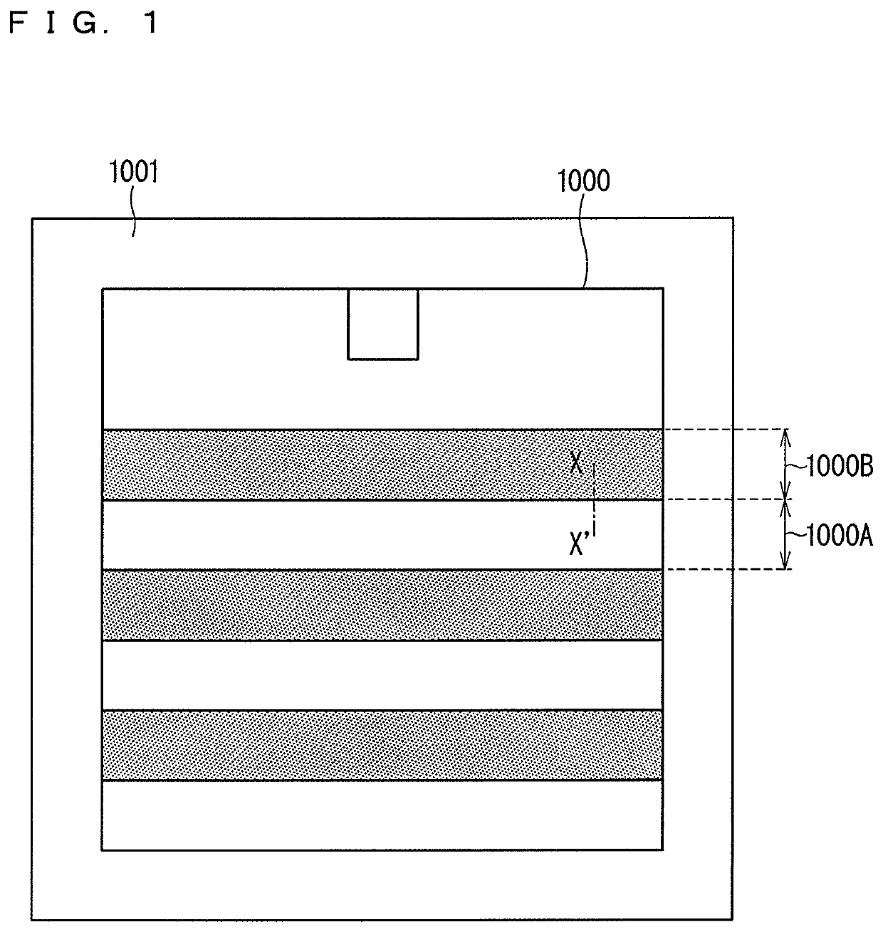
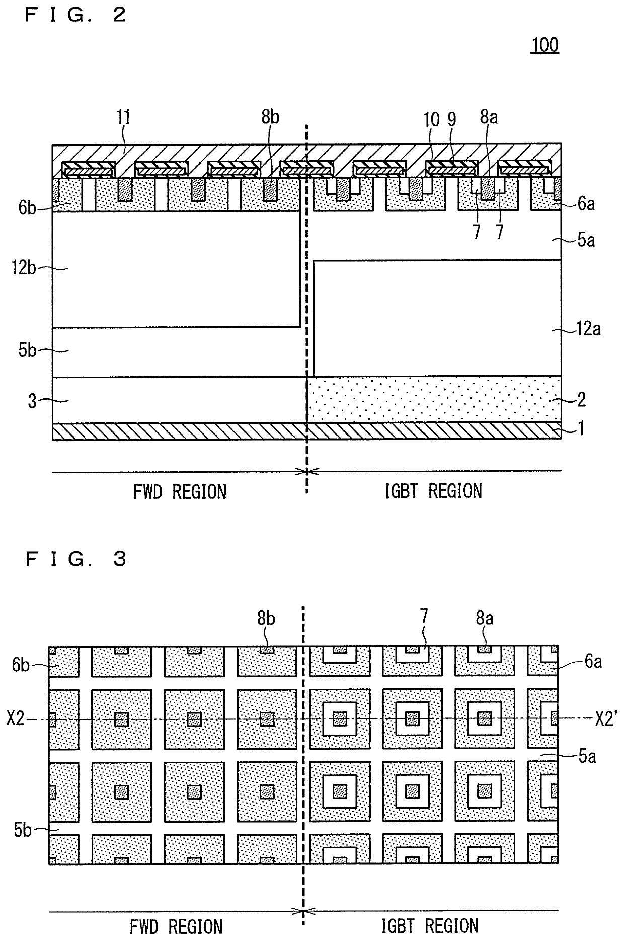
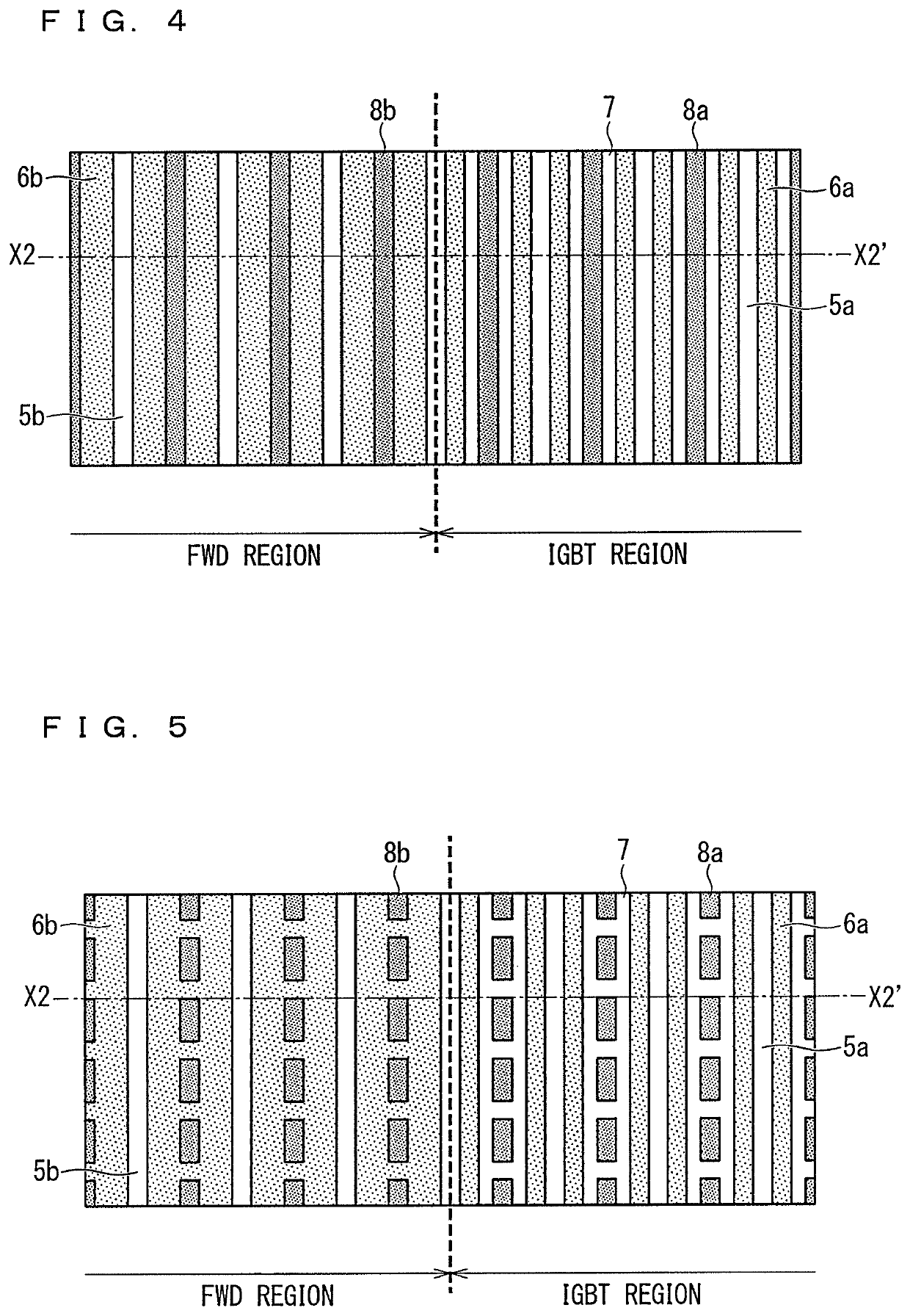
[0076]FIG. 1 is a plan view schematically showing an example of a configuration of a semiconductor device (specifically, a planar gate type SiC-RC-IGBT) according to the present embodiment.

[0077]As shown in FIG. 1, the SiC-RC-IGBT includes an active region ...

second embodiment

[0204]A semiconductor device according to the present embodiment will be described. It should be noted that in the following description, the same components as those described in the embodiment described above are denoted by the same reference numerals and illustrated, and the detailed description thereof will be appropriately omitted.

[0205]

[0206]FIG. 18 is a cross-sectional view schematically showing an example of a configuration of a semiconductor device (specifically, a trench gate type SiC-RC-IGBT) according to the present embodiment. As shown with an example in FIG. 18, the semiconductor device according to the present embodiment is similar in configuration to the semiconductor device according to the first embodiment. Therefore, in the present embodiment, in particular, portions different from the configuration of the semiconductor device in the first embodiment will be described.

[0207]As shown with an example in FIG. 18, an IGBT region of a SiC-RC-IGBT 200 includes: an n-typ...

third embodiment

[0213]A semiconductor device according to the present embodiment will be described. It should be noted that in the following description, the same components as those described in the embodiments described above are denoted by the same reference numerals and illustrated, and the detailed description thereof will be appropriately omitted.

[0214]FIG. 19 is a cross-sectional view schematically showing an example of a configuration of a semiconductor device (specifically, a planar gate type SiC-RC-IGBT) according to the present embodiment. As shown with an example in FIG. 19, the semiconductor device according to the present embodiment is similar in configuration to the semiconductor device according to the first embodiment. Therefore, in the present embodiment, in particular, portions different from the configuration of the semiconductor device in the first embodiment will be described.

[0215]As shown with an example in FIG. 19, an IGBT region of a SiC-RC-IGBT 300 includes: an n-type dri...


PUM


Abstract

In order to improve energization capacity, minority carrier injection efficiency is increased. In a semiconductor device, an IGBT includes a first drift layer, a collector region, a base region, an emitter region, an insulating film, a gate electrode, and a first high carrier lifetime region formed at a position closer to the collector region than the base region and having a longer carrier lifetime than the first drift layer. An FWD includes a second drift layer, an anode region, and a second high carrier lifetime region formed at a position closer to the anode region than a lower surface of the second drift layer and having a longer carrier lifetime than the second drift layer.

Description

TECHNICAL FIELD[0001]The technique disclosed in the specification of the present application relates to a semiconductor device and a method for manufacturing the semiconductor device.BACKGROUND ART[0002]Conventionally, there has been known a power semiconductor device in which an insulated gate bipolar transistor, that is, IGBT using silicon (Si) as a semiconductor material and a free-wheeling diode, that is, FWD connected in antiparallel with the IGBT are formed in the same semiconductor substrate.[0003]For example, Patent Document 1 discloses a semiconductor device in which an IGBT and an FWD are formed on the same semiconductor substrate, a common electrode functioning as an emitter electrode of the IGBT and an anode electrode of the FWD is formed on an upper surface side of the semiconductor substrate, and a common electrode functioning as a collector electrode of the IGBT and a cathode electrode of the FWD is formed on a lower surface side of the semiconductor substrate.[0004]S...

Claims


Application Information

Patent Timeline
IPC IPC(8): H01L27/06H01L29/06H01L29/739H01L29/66
CPCH01L27/0629H01L29/66333H01L29/7394H01L29/0696H01L29/78H01L29/7395H01L29/32H01L29/7397H01L29/8611H01L29/407H01L29/66136H01L29/1608H01L27/0727
Inventor HAMADA, KENJIKONISHI, KAZUYAKAWAHARA, KOTARO
Owner MITSUBISHI ELECTRIC CORP
Why Eureka
Try Eureka