

Laminating process of multi-layer circuit board
A multi-layer circuit board and lamination process technology, which is applied in multi-layer circuit manufacturing, printed circuit, printed circuit manufacturing, etc., can solve problems such as defects in the electrical conductivity of circuit boards, avoid delamination and explosion boards, and increase the electrification rate , enhance the binding effect
- Summary
- Abstract
- Description
- Claims
- Application Information
AI Technical Summary
Problems solved by technology
Method used
Image

Examples
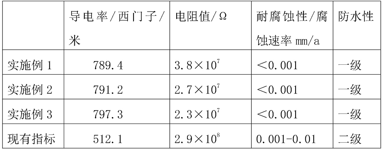
Embodiment 1
[0023] A lamination process for a multilayer circuit board, the process comprising:
[0024] (1) Pre-machine: Preheat the laminator to a temperature of 130°C;
[0025] (2) Component preparation: Lay single-layer circuit board, thermosetting adhesive film, graphene sheet, thermosetting adhesive film, single-layer circuit board, thermosetting adhesive film, graphene sheet, thermosetting adhesive film, layer circuit board to form a multi-layer circuit board assembly;
[0026] (3) Negative pressure lamination stage: open the laminator, place the prepared circuit board assembly in the laminator, then close the lid of the laminator, vacuum the upper chamber of the laminator, and vacuum the upper chamber of the laminator, Keep the vacuum at -75kpa, the process lasts for 30s, the lower chamber of the laminator starts to vacuum, keep the vacuum at -58kpa, and last for 200s;
[0027] (4) Positive pressure lamination stage: the upper chamber of the laminator starts to inflate, and the ...
Embodiment 2
[0032] A lamination process for a multilayer circuit board, the process comprising:
[0033] (1) Pre-machine: Preheat the laminator to a temperature of 130°C;
[0034] (2) Component preparation: Lay single-layer circuit board, thermosetting adhesive film, graphene sheet, thermosetting adhesive film, single-layer circuit board, thermosetting adhesive film, graphene sheet, thermosetting adhesive film, layer circuit board to form a multi-layer circuit board assembly;
[0035] (3) Negative pressure lamination stage: open the laminator, place the prepared circuit board assembly in the laminator, then close the lid of the laminator, vacuum the upper chamber of the laminator, and vacuum the upper chamber of the laminator, Keep the vacuum at -75kpa, the process lasts for 30s, the lower chamber of the laminator starts to vacuum, keep the vacuum at -70kpa, and last for 220s;
[0036] (4) Positive pressure lamination stage: the upper chamber of the laminator starts to inflate, and the ...
Embodiment 3
[0041] A lamination process for a multilayer circuit board, the process comprising:
[0042] (1) Pre-machine: Preheat the laminator to a temperature of 130°C;
[0043](2) Component preparation: Lay single-layer circuit board, thermosetting adhesive film, graphene sheet, thermosetting adhesive film, single-layer circuit board, thermosetting adhesive film, graphene sheet, thermosetting adhesive film, layer circuit board to form a multi-layer circuit board assembly;
[0044] (3) Negative pressure lamination stage: open the laminator, place the prepared circuit board assembly in the laminator, then close the lid of the laminator, vacuum the upper chamber of the laminator, and vacuum the upper chamber of the laminator, Keep the vacuum at -75kpa, the process lasts for 30s, the lower chamber of the laminator starts to vacuum, keep the vacuum at 90kpa, and last for 250s;
[0045] (4) Positive pressure lamination stage: the upper chamber of the laminator starts to inflate, and the mo...
PUM
 Abstract
Description
Claims
Application Information