Screen printing plate structure of monocrystalline silicon solar cell

A solar cell and monocrystalline silicon technology, applied in the field of solar cells, can solve the problems of positive electrode current conduction affecting the whole cell, easy cracking and breaking of the edge of the cell, large shading area of ​​the positive electrode, etc. Metal conduction resistance, avoiding easy cracking and breaking, reducing the effect of damage probability

Pending Publication Date: 2020-01-17
TONGWEI SOLAR ENERGY MEISHAN CO LTD
View PDF0 Cites 1 Cited by
  • Summary
  • Abstract
  • Description
  • Claims
  • Application Information

AI Technical Summary

Problems solved by technology

[0006] The purpose of the present invention is: in order to solve the problem that the positive electrode shading area of ​​the existing monocrystalline silicon solar cell is too large, resulting in low efficiency, the edge of the cell is easy to be cracked and broken after the two ends of the main grid line of the positive electrode are welded, and the breakage of the auxiliary grid line will affect To solve the technical problem of the positive electrode current conduction of the whole cell, the present invention provides a screen structure of a monocrystalline silicon solar cell

Method used


Image

  • Screen printing plate structure of monocrystalline silicon solar cell
  • Screen printing plate structure of monocrystalline silicon solar cell
  • Screen printing plate structure of monocrystalline silicon solar cell

Examples


Embodiment 1

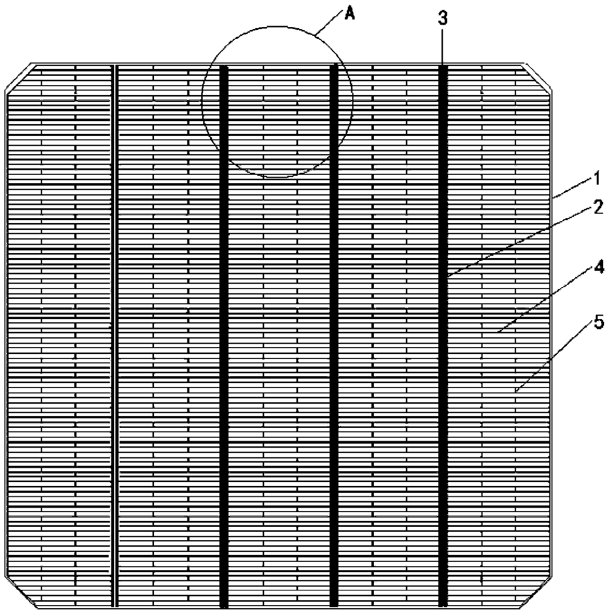
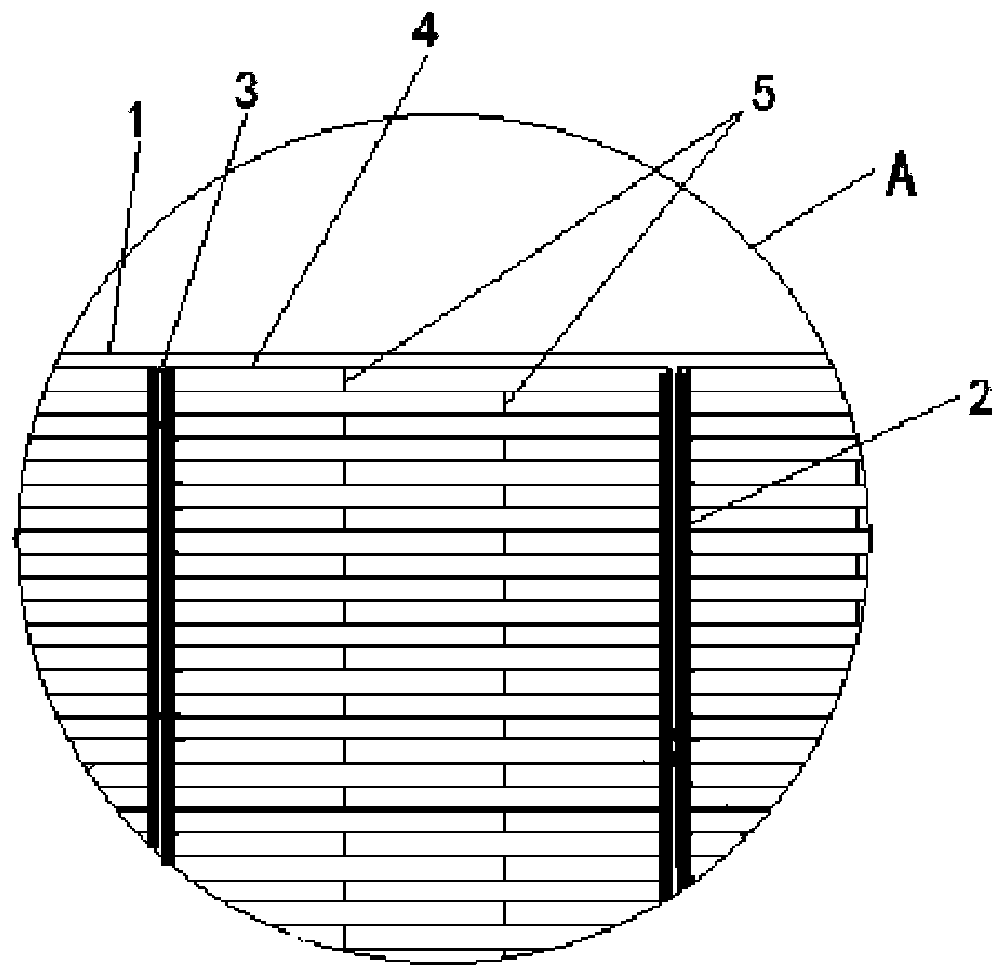
[0033] Such as Figure 1 to 2 As shown, this embodiment provides a mesh structure of a monocrystalline silicon solar cell, which includes a cell 1 with a number of front electrode regions on the front of the cell 1, and bus bars 2 between adjacent front electrode regions. The middle of the main grid line 2 is provided with a partition 3, the main grid line 2 is vertically connected with a number of sub-grid lines 4 located in the front electrode area, and both ends of the main grid line 2 are connected to the outermost sub-grid line 4, adjacent sub-grid lines 4 An anti-breakage grid line 5 is connected between the grid lines 4.

[0034] In this embodiment, the front side of the cell (that is, the positive electrode) adopts a partition structure, where it can generally be divided into 5 front electrode areas, and a partition area is provided in the middle of the main grid line to ensure the collection of photo-generated carriers and the assembly On the basis of welding reliability...

Embodiment 2

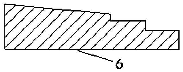
[0040] Such as Figure 1 to 4 As shown, this embodiment is further optimized on the basis of Embodiment 1. Specifically, a contact extension 6 is connected between the main gate line 2 and the auxiliary gate line 4, and the height of the contact extension 6 is greater than that of the auxiliary gate. The height of the wire 4, the contact extension 6 gradually narrows from the end close to the bus line 2 to the end far away from the bus line 2.

[0041] The length of the contact extension 6 is 0.3-0.7 mm, the width of the end of the contact extension 6 close to the bus line 2 is 0.6 mm, and the width of the end of the contact extension 6 away from the bus line 2 is 0.3 mm.

[0042] In this embodiment, the contact extension section can prevent the sub-gate line and the main gate line from being broken. In addition, when the collected conduction current in this area is concentrated to the maximum, the slurry of the contact extension section is superimposed in the height direction to ex...

Embodiment 3

[0044] Such as Figure 5 to 6 As shown, this embodiment is further optimized on the basis of embodiment 1. Specifically, the back of the battery sheet 1 is provided with a plurality of longitudinally arranged strip hollow areas 7 at positions corresponding to the front electrode area, where the strip hollow areas 7 Each column can be set up to 4 to form a 4X5 square array of strip hollow areas 7 as a whole. The strip hollow areas 7 are embedded with hollow electrodes 8, and both ends of the hollow electrodes 8 are connected vertically. Strip pins 9 arranged at equal intervals.

[0045] In this embodiment, a number of strip hollow areas are opened on the back of the cell, and hollow electrodes are nested and printed, and a number of strip pins are arranged on the edges of the hollow electrodes to ensure the basis for the overlap between the back of the cell (ie, the back electric field) and the hollow electrodes The upper part reduces the overlap area of ​​the paste, reduces the ...


PUM

PropertyMeasurementUnit
widthaaaaaaaaaa
lengthaaaaaaaaaa
lengthaaaaaaaaaa

Abstract

The invention discloses a screen printing plate structure of a monocrystalline silicon solar cell, and relates to the technical field of solar cells. The screen printing plate structure comprises a cell piece, the right side of the cell piece is provided with a plurality of front electrode areas, and the main grid lines are arranged between the adjacent front electrode areas. Partition areas are arranged in the middles of the main grid lines, the main grid lines are vertically connected with a plurality of auxiliary grid lines positioned in the front electrode areas, the two tail ends of the main grid lines are both connected with the outermost auxiliary grid line, and the break-proof grid lines are connected between the adjacent f auxiliary grid lines. The screen printing plate structurehas the advantages that the shading area can be reduced, the cell efficiency can be improved, meanwhile, the problem that the edge of the cell piece is prone to subfissure and breakage can be avoided,and the current collection of the whole cell piece cannot be affected when the auxiliary grid lines are broken.

Description

Technical field [0001] The invention relates to the technical field of solar cells, and more specifically to a screen structure of a monocrystalline silicon solar cell. Background technique [0002] With the rapid development of crystalline silicon photovoltaic technology, the expansion of solar cell production scale and the drive of inherent quality benefits, how to reduce costs and improve efficiency has become the top priority of large-scale battery production. At present, the most common crystalline silicon solar cells include monocrystalline silicon solar cells, polycrystalline silicon solar cells and amorphous silicon solar cells. Quasi-single crystal or similar monocrystalline cells are solar cells on a common substrate between monocrystalline silicon and polycrystalline silicon. Among them, more than 90% of crystalline silicon solar cells use screen printing technology to make the metal paste and the silicon substrate contact, thereby deriving the photo-generated current ...

Claims


Application Information

Patent Timeline
Patent Type & Authority Applications(China)
IPC IPC(8): H01L31/0224
CPCH01L31/022425Y02E10/50
Inventor 王岚李忠涌杨蕾陈明张忠文谢毅
Owner TONGWEI SOLAR ENERGY MEISHAN CO LTD
Why Eureka
Try Eureka