A structure to enhance the contact strength of electronic circuit surface

An electronic circuit, surface contact technology, applied in the field of communication, can solve the problems of unstable electrical performance, contact failure, large contact resistance, etc., and achieve the effect of reducing unnecessary steps, improving performance stability, and reducing conductive resistance.

Inactive Publication Date: 2017-03-29
SHANGHAI AMPHENOL AIRWAVE COMM ELECTRONICS CO LTD
View PDF4 Cites 1 Cited by
  • Summary
  • Abstract
  • Description
  • Claims
  • Application Information

AI Technical Summary

Problems solved by technology

[0003] In the current mobile terminal products, especially in the production of the circuit (PPA, PadPrint Antenna) made by printing conductive ink, the material of the electronic circuit used is generally made of nano-silver. The electronic circuits produced by it are easily damaged when they come into contact with the contact points on the main board of the mobile terminal, resulting in failure of the contact between the electronic circuit and the main board
[0004] However, in conventional products of the prior art, in order to solve the problem of contact failure of the circuit (PPA) made by pad printing conductive ink, it is generally here In this contact method, a soft conductive material is used to connect the two, such as using conductive foam to connect the two. However, although this connection method can avoid damage to the electronic circuit when the two are in contact, because the conductive foam is connected, The contact resistance between each other is large, and the electrical performance is unstable, which is not conducive to the reliable transmission of communication signals
[0005] Therefore, it is necessary to propose a structure that strengthens the surface contact strength of electronic circuits to solve a series of effects caused by poor contact of electronic circuits in the prior art

Method used


Image

  • A structure to enhance the contact strength of electronic circuit surface
  • A structure to enhance the contact strength of electronic circuit surface
  • A structure to enhance the contact strength of electronic circuit surface

Examples


Embodiment 1

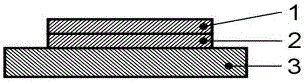
[0024] Such as figure 1 As shown, the first structure provided by the present invention to strengthen the surface contact strength of electronic circuits is used in a communication product. The structure includes an electronic circuit body 3, conductive glue or conductive double-sided tape 2 and a metal sheet 1, wherein the electronic circuit The circuit body 3 is a printed electronic circuit, including a laser direct structuring (LDS) circuit, a flexible circuit board or a circuit (PPA) made of pad printing conductive ink; conductive glue or conductive double-sided tape 2 is a reinforcing material with good conductivity The metal sheet 1 is a conductive material with good strength and toughness, including stainless steel sheet, copper sheet or other metal sheets with good conductivity; The two are connected and fixed to form an integral body, so that the electronic circuit body 3 is connected with the spring pins or pins on the main board, and the damage of the electronic cir...

Embodiment 2

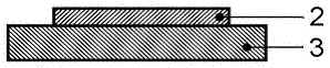
[0029] Such as figure 2 As shown, the second structure for strengthening the contact strength of the electronic circuit surface provided by the present invention includes an electronic circuit body 3 and a conductive glue or a conductive double-sided adhesive tape 2, wherein the electronic circuit body 3 is a printed electronic circuit, including Laser Direct Structuring (LDS) circuits, flexible circuit boards or circuits made of pad printing conductive ink (PPA), conductive glue or conductive double-sided tape 2 are conductive materials with good conductivity; by applying conductive glue or conductive double-sided tape 2 Uniformly cover the surface of the electronic circuit body 3 to solidify the two into one body, thereby connecting the electronic circuit body 3 with the spring pins or spring pins on the main board, and avoiding damage to the electronic circuit body 3 .

[0030] Wherein, the specific steps of the manufacturing method of the structure having two layers of el...

Embodiment 3

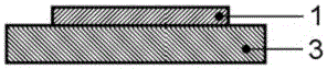
[0034] Such as image 3 As shown, the present invention proposes a third structure for strengthening the contact strength of the electronic circuit surface, which is used in a communication product. The strengthening structure includes an electronic circuit body 3 and a metal sheet 1, wherein the electronic circuit body 3 is a printed electronic circuit , or a circuit (PPA) made of pad printing conductive ink, the metal sheet 1 is a conductive material with good toughness, such as a stainless steel sheet, copper sheet or other metal sheets with good conductivity; the electronic circuit body made of nano-silver 3 is relatively soft, and before the electronic circuit body 3 is cured, the metal sheet is evenly covered on the electronic circuit body 3, and after curing, the two are combined to form a whole, so as to realize the connection of other components of the electronic circuit body 3 and avoid the electronic circuit Damage to body 3.

[0035] Wherein, the specific steps of...


PUM


Abstract

The invention discloses a structure for strengthening surface contract strength of an electronic circuit. The structure is used in communication products. The structure comprises an electronic circuit body and strengthening materials evenly coating the electronic circuit body, and the electronic circuit body is connected with a main board through the strengthening materials. The strengthening materials of the structure for strengthening the surface contract strength of the electronic circuit can be metal sheets, conductive double sticky tape and conductive glue respectively, the strengthening materials can also be in the mode of combining the metal sheets and the conductive double sticky tape, conductive glue or combining the metal sheets and the conductive glue, the metal sheets are fixedly connected with the electronic circuit body through the conductive double sticky tape or the conductive glue, and therefore the electronic circuit body is not damaged when connected with other parts, and the contact stability of the structure is greatly improved.

Description

technical field [0001] The invention relates to the communication field, in particular to a structure for strengthening the surface contact strength of an electronic circuit. Background technique [0002] With the rapid development of communication technology, the update of the antenna part is very rapid, from external to internal, among which, the preparation of metal shrapnel antenna, FPC / PCB antenna, printed antenna and LDS (Laser Direct structuring, laser direct structuring) antenna more and more. Especially with the rapid development of wireless communication in recent years, mobile terminals occupy a dominant position. In particular, mobile terminals are gradually developing toward miniaturization and intelligence, and communication antennas as mobile terminals have become extremely important. [0003] In the current mobile terminal products, especially in the production of the circuit (PPA, PadPrint Antenna) made by printing conductive ink, the material of the elect...

Claims


Application Information

Patent Timeline
Patent Type & Authority Patents(China)
IPC IPC(8): H05K1/02H05K1/09
Inventor 郑兵陈德智熊新刚
Owner SHANGHAI AMPHENOL AIRWAVE COMM ELECTRONICS CO LTD
Why Eureka
Try Eureka