Nitride semiconductor element, nitride semiconductor light emitting element, ultraviolet light emitting element

a technology of semiconductor elements and light emitting elements, applied in the field of nitride semiconductor elements, can solve the problems of reduced resistance and need for further reduction of contact resistance, and achieve the effects of improving the efficiency of carrier high efficiency of the light emitting element 10a, and improving the efficiency of hole injection into the light emitting layer

Active Publication Date: 2019-05-09
ASAHI KASEI KK
View PDF3 Cites 0 Cited by
  • Summary
  • Abstract
  • Description
  • Claims
  • Application Information

AI Technical Summary

Benefits of technology

[0150]In the ultraviolet light emitting element 10A of the second embodiment, the carrier injection efficiency into a light emitting layer improves by including an AlxGa(1-x)N layer having an Al composition x of 0.90 or more and 1.00 or less with a film thickness of 5 nm or more and 18 nm or less as the carrier blocking layer 330, and therefore high efficiency of the light emitting element 10A is obtained.
[0152]In the ultraviolet light emitting element 10A of the second embodiment, the hole injection efficiency into a light emitting layer improves due to the presence of the graded layer 340 having a film thickness of 5 nm or more and 110 nm or less, and therefore high efficiency of the light emitting element is obtained.
[0154]The ultraviolet light emitting element 10A of the second embodiment contains an n-AlxGa(1-x)N layer having a high Al composition x of 0.50 or more and less than 0.80 as the n-type Group III semiconductor layer 2. Due to the presence of both an aluminum substance and an alloy containing aluminum and nickel in the contact surface 41 or in the vicinity of the contact surface 41 to the n-type semiconductor layer 2 of the first electrode layer 4, a contact resistance can be greatly reduced. Since the contact resistance is reduced, a forward voltage of the ultraviolet light emitting element 10A can be lowered, and therefore the heat generation amount of the ultraviolet light emitting element 10A can be reduced. Accordingly, an optical power output becomes high and / or lifetime becomes longer because the amount of heat generation in the ultraviolet light emitting element 10A is reduced.
[0155]Because the amount of heat generation in the ultraviolet light emitting element 10A is reduced, smaller size of heat sink for the nitride semiconductor light emitting device containing the ultraviolet light emitting element 10A can be applied, and therefore a size reduction of the nitride semiconductor light emitting device is achieved.
[0156]Furthermore, in the ultraviolet light emitting element 10A of the second embodiment, the aluminum substance present in the contact surface 41 or in the vicinity of the contact surface 41 to the n-type Group III nitride semiconductor layer which means a high conductivity layer is formed on or near the interface to the n-type Group III nitride semiconductor layer 20 of the first electrode layer 4. Therefore, a current can be easily spread in the lateral direction of the first electrode layer 4 so that contact resistance can be reduced and / or current crowding can be mitigated. Moreover, since the reflectance on or near the interface with the n-type Group III nitride semiconductor layer 20 of the first electrode layer 4 can be increased by the aluminum substance exists, the optical power output can be increased. Although the effects mentioned above can be obtained also by aluminum in an alloy containing the aluminum, the effects obtained by the aluminum substance are higher.
[0157]Moreover, in the ultraviolet light emitting element 10A of the second embodiment, the alloy containing aluminum and nickel is present in the contact surface 41 or in the vicinity of the contact surface 41 to the n-type Group III nitride semiconductor layer 20 of the first electrode layer 4. Such a first electrode layer 4 can be formed under the condition where the alloy containing aluminum and nickel is easily formed, e.g., under the condition where a high resistance alloy, such as an alloy of aluminum and gold, is harder to be formed. As a result, the formation of the high resistance alloy is reduced, and therefore a contact resistance reduction effect is obtained.

Problems solved by technology

According to the method described in PTL 1, a contact resistance is reduced but insufficient, and thus further reduction of the contact resistance is necessary.

Method used


Image

  • Nitride semiconductor element, nitride semiconductor light emitting element, ultraviolet light emitting element
  • Nitride semiconductor element, nitride semiconductor light emitting element, ultraviolet light emitting element
  • Nitride semiconductor element, nitride semiconductor light emitting element, ultraviolet light emitting element

Examples


embodiments

[0059]Hereinafter, embodiments of the present invention are described but the present invention is not limited to the embodiments described below. The embodiments described below include technically preferable limitations to carry out the present invention but the limitations are not indispensable requirements of the present invention.

first embodiment

[0060]A first embodiment describes an example in which the nitride semiconductor element of the first aspect of the present invention is applied to an ultraviolet light emitting element.

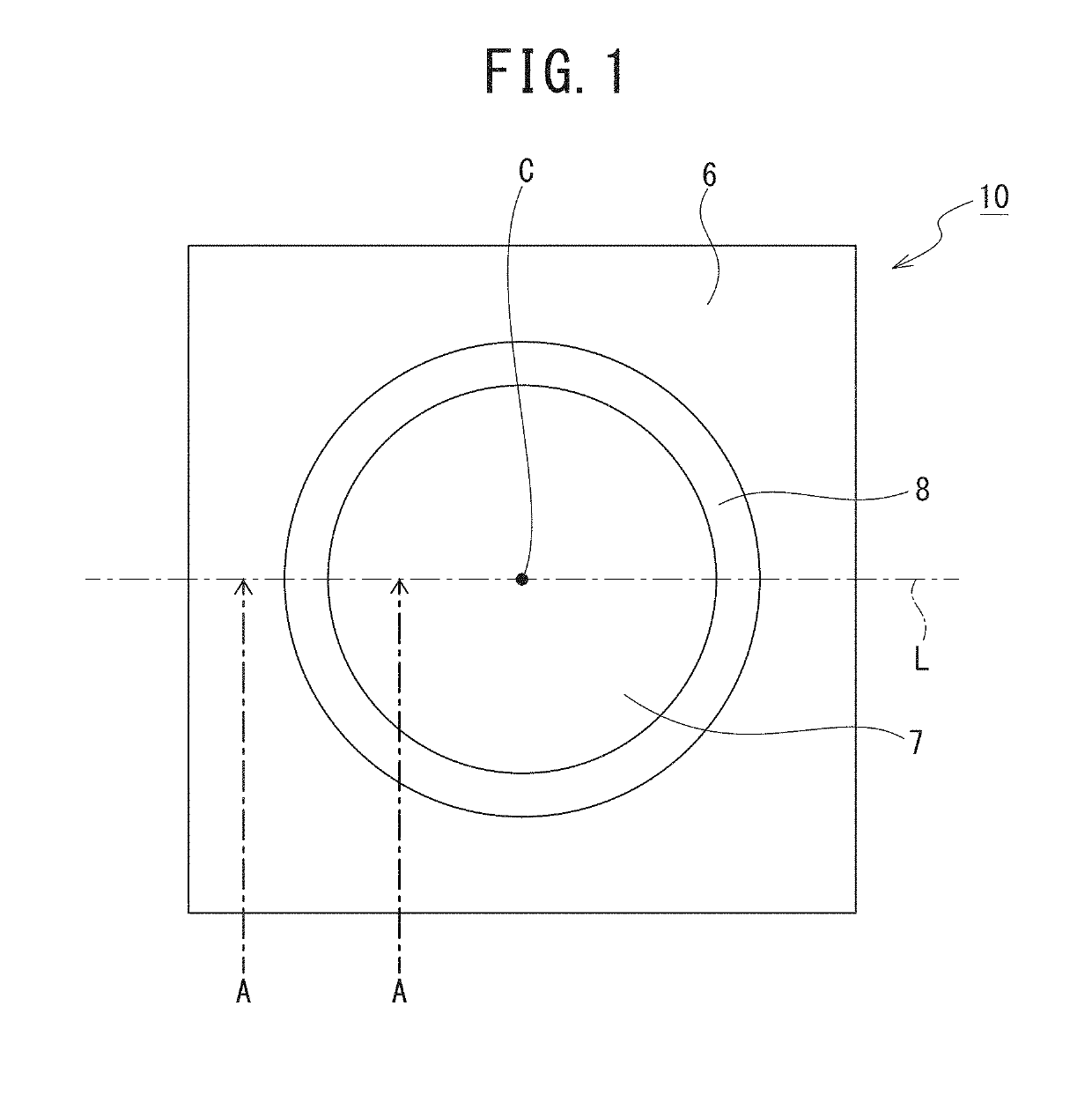
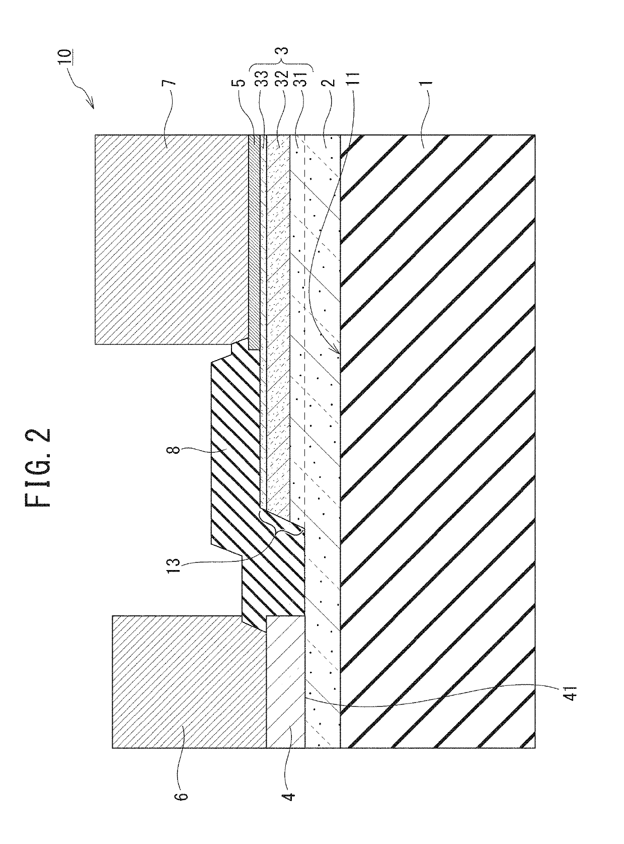
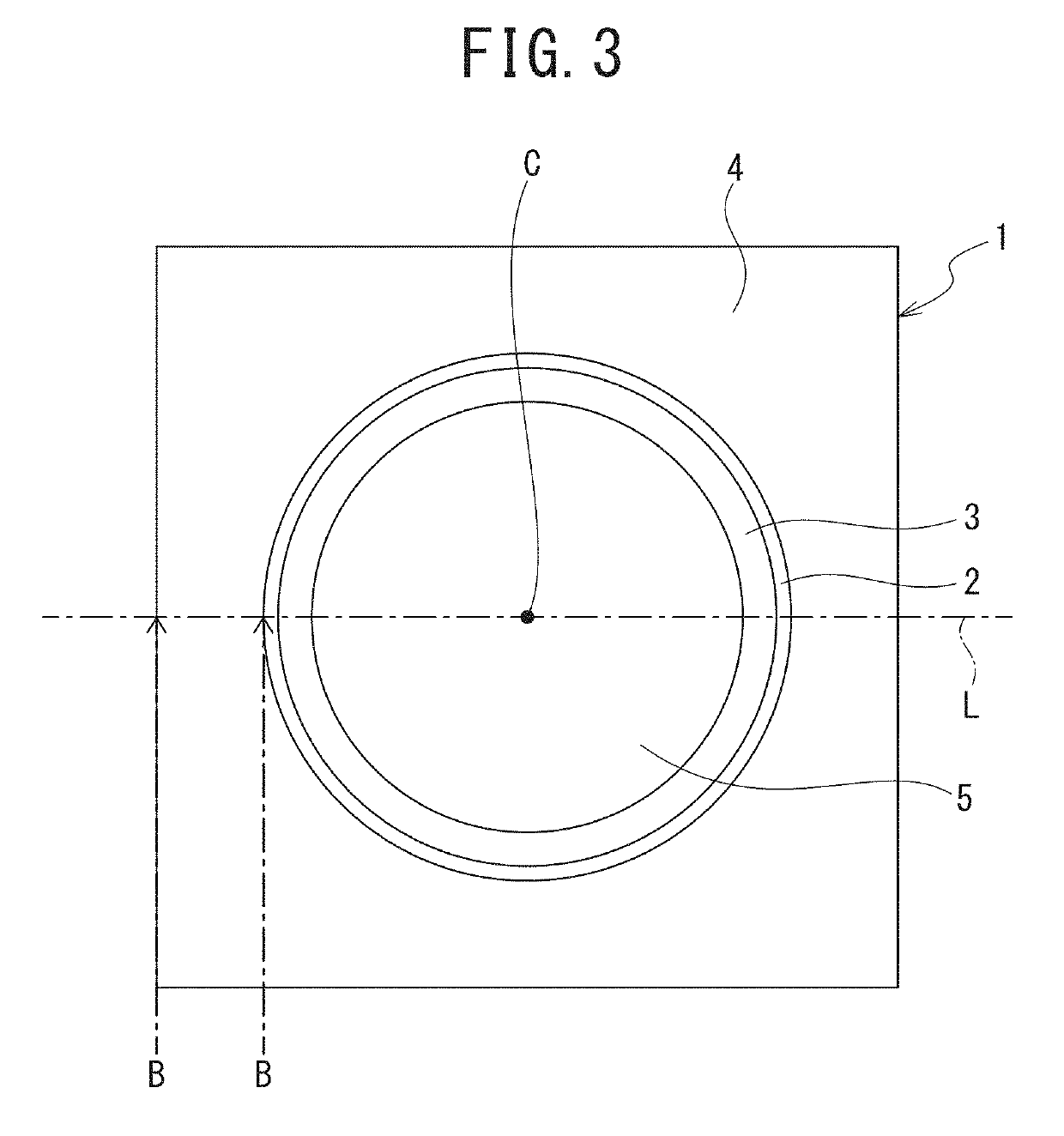
[0061]First, the entire configuration of an ultraviolet light emitting element 10 of this embodiment is described with FIG. 1 to FIG. 3.

[0062]As illustrated in FIG. 1 and FIG. 2, the ultraviolet light emitting element 10 has a substrate 1, an n-type nitride semiconductor layer (first conductivity type first nitride semiconductor layer) 2, a nitride semiconductor body 3, a first electrode layer 4, a second electrode layer 5, a first pad electrode 6, a second pad electrode 7, and an insulation layers 8.

[0063]The n-type nitride semiconductor layer 2 is formed on one surface 11 of the substrate 1. The nitride semiconductor body 3 is a mesa portion formed in a part on the n-type nitride semiconductor layer 2 and has a side surface 13 which is inclined. As illustrated in FIG. 2, the nitride semiconductor b...

second embodiment

[0105]A second embodiment describes an example in which the nitride semiconductor light emitting element of the second aspect of the present invention is applied to an ultraviolet light emitting element. The conductivity type of a first Group III nitride semiconductor layer is set to an n-type and the conductivity type of a second Group III nitride semiconductor layer is set to a p-type.

[0106]First, the entire configuration of an ultraviolet light emitting element 10A of this embodiment is described with FIG. 7 and FIG. 8.

[0107]As illustrated in FIG. 7, the ultraviolet light emitting element 10A has a substrate 1, an n-type Group III nitride semiconductor layer (first Group III nitride semiconductor layer) 20, a nitride semiconductor body 30, a first electrode layer 4, a second electrode layer 5, a first pad electrode 6, a second pad electrode 7, and an insulation layers 8. The n-type Group III nitride semiconductor layer 20 is formed on the substrate 1. The nitride semiconductor bo...


PUM


Abstract

To provide a nitride semiconductor element having a better contact resistance reduction effect also in the case of a light emitting element containing AlGaN having a high Al composition. The nitride semiconductor element has a substrate 1, a first conductivity type first nitride semiconductor layer 2 formed on the substrate 1, and a first electrode layer 4 formed on the first nitride semiconductor layer 2. The first electrode layer 4 contains aluminum and nickel, and both aluminum and an alloy containing aluminum and nickel are present in a contact surface to the first nitride semiconductor layer 2 or in the vicinity of the contact surface.

Description

BACKGROUND OF THE INVENTIONField of the Invention[0001]The present invention relates to a nitride semiconductor element.Description of the Related Art[0002]Nitride semiconductors, such as AlN, GaN, InN, and AlGaN, are attractive materials capable of variously changing the energy band gap by changing the composition ratio of Group III elements (Al, Ga, In).[0003]In particular, AlGaN has been used for various devices, such as deep UV sensors / light emitting diodes and AlGaN / GaN power devices and transistors. However, AlGaN having a high Al composition is well known as difficult to form an ohmic contact with electrode materials, and thus causing an increase in resistance of AlGaN / electrode interface. Moreover, an electrode contains several metal materials and necessary to be annealed in order to make good contact with AlGaN, and therefore alloys can be formed during the annealing process. When the resistance of the formed alloys is high, the bulk resistance of the electrode increases in...

Claims


Application Information

Patent Timeline
Patent Type & Authority Applications(United States)
IPC IPC(8): H01L33/32H01L33/06H01L33/40
CPCH01L33/325H01L33/06H01L33/40H01L33/32H01L33/20H01L2933/0016
Inventor YOKOYAMA, AYAHAGIHARA, YOSHIHITOHASEGAWA, RYOSUKEYOSHIKAWA, AKIRAZHANG, ZIYIMORISHITA, TOMOHIRO
Owner ASAHI KASEI KK
Why Eureka
Try Eureka