
Method of manufacturing flash memory device

Inactive Publication Date: 2010-09-09
EON SILICON SOLUTION
View PDF2 Cites 0 Cited by
  • Summary
  • Abstract
  • Description
  • Claims
  • Application Information

AI Technical Summary

Benefits of technology

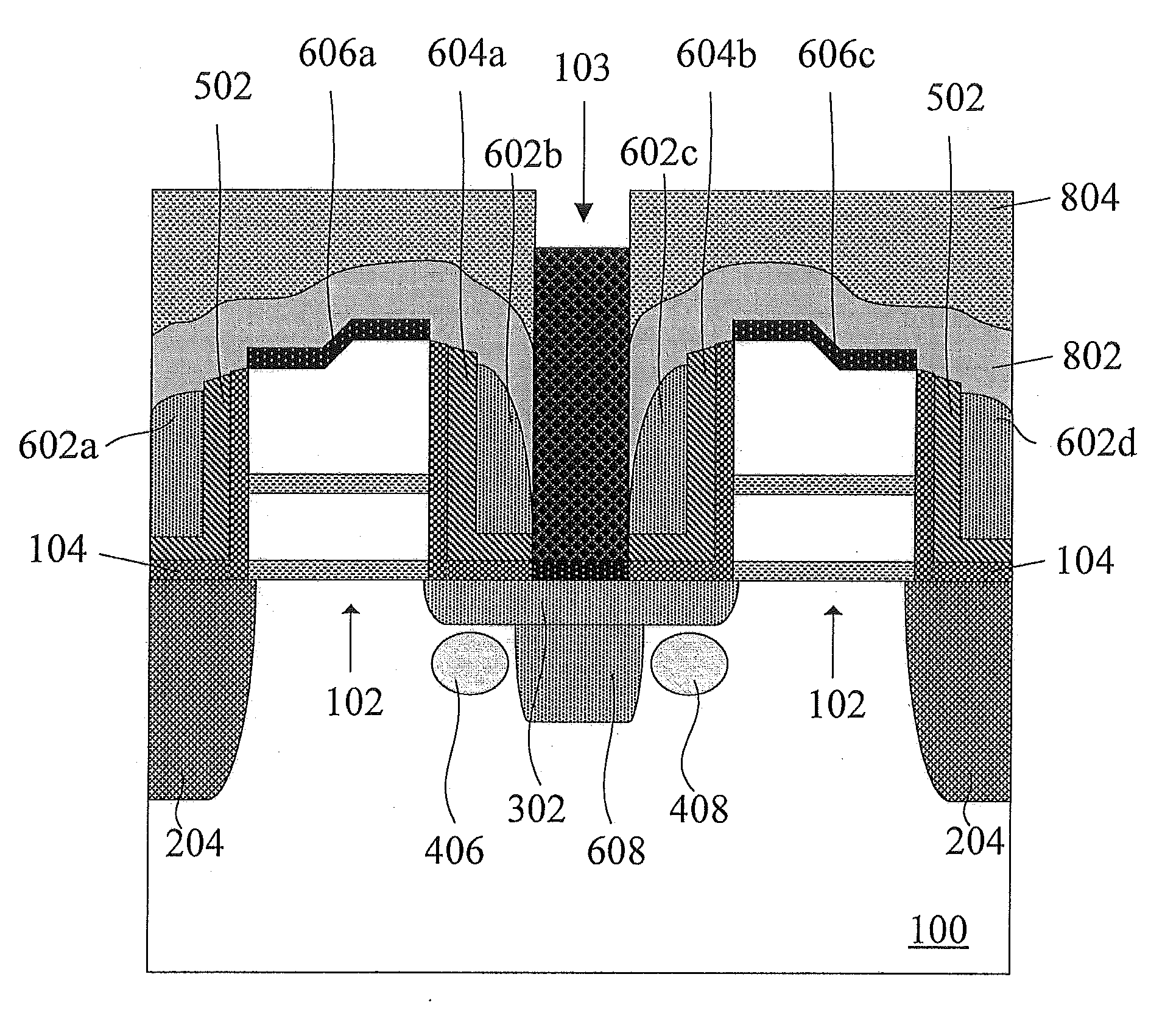
[0005]A primary object of the present invention is to provide a method of manufacturing a flash memory device, so that hot carriers are generated closer to junctions of drains in a semiconductor substrate to thereby enable enhanced hot carrier injection efficiency, which in turn reduces the drain voltage to improve the short channel effects (SCE).
[0007]With the flash memory device manufacturing method of the present invention, the drain voltage can be lowered, and the short channel effects can be improved through the pocket implantation process.

Problems solved by technology

However, the movement of the memory devices into the nanometer era also brings the problems of short channel effects (SCE) and gate leakage current.
As a result, it becomes more difficult to enhance the memory device performance by reducing the channel length and gate oxide layer thickness of the memory device.
While the lightly doped drain reduces the high electric field at the drain junction and effectively upgrades the reliability of the device, the punch-through phenomena becomes worse when the device dimensions are gradually reduced.
While the pocket implantation improves the short channel effects of the device, the phenomena of drain current (IDSAT) degradation will occur due to high channel doping.

Method used


Image

  • Method of manufacturing flash memory device
  • Method of manufacturing flash memory device
  • Method of manufacturing flash memory device

Examples


Embodiment Construction

[0010]The present invention will now be described with a preferred embodiment thereof. For the purpose of easy to understand, elements that are the same in the illustrated preferred embodiment and the accompanying drawings are denoted by the same reference numerals.

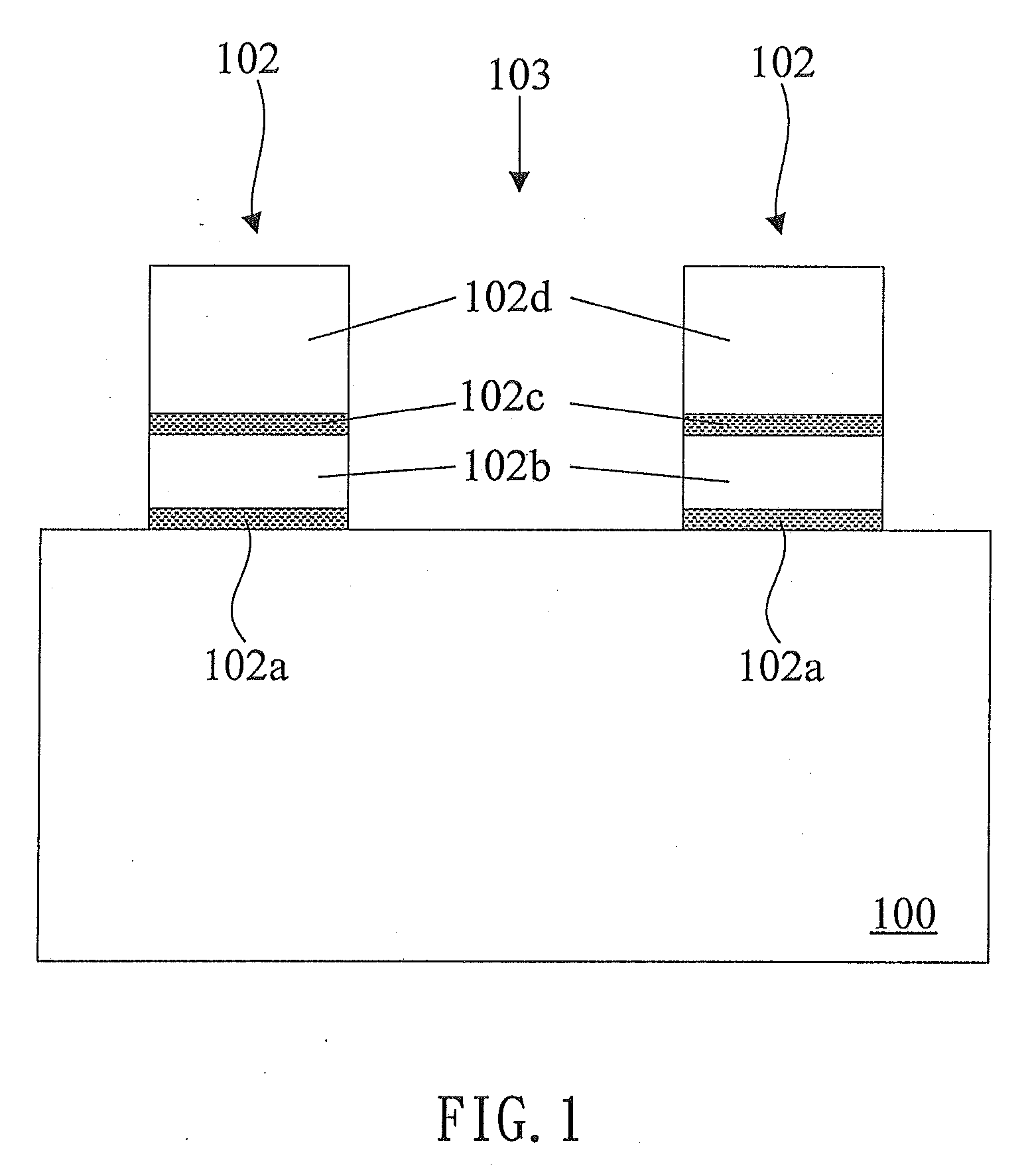
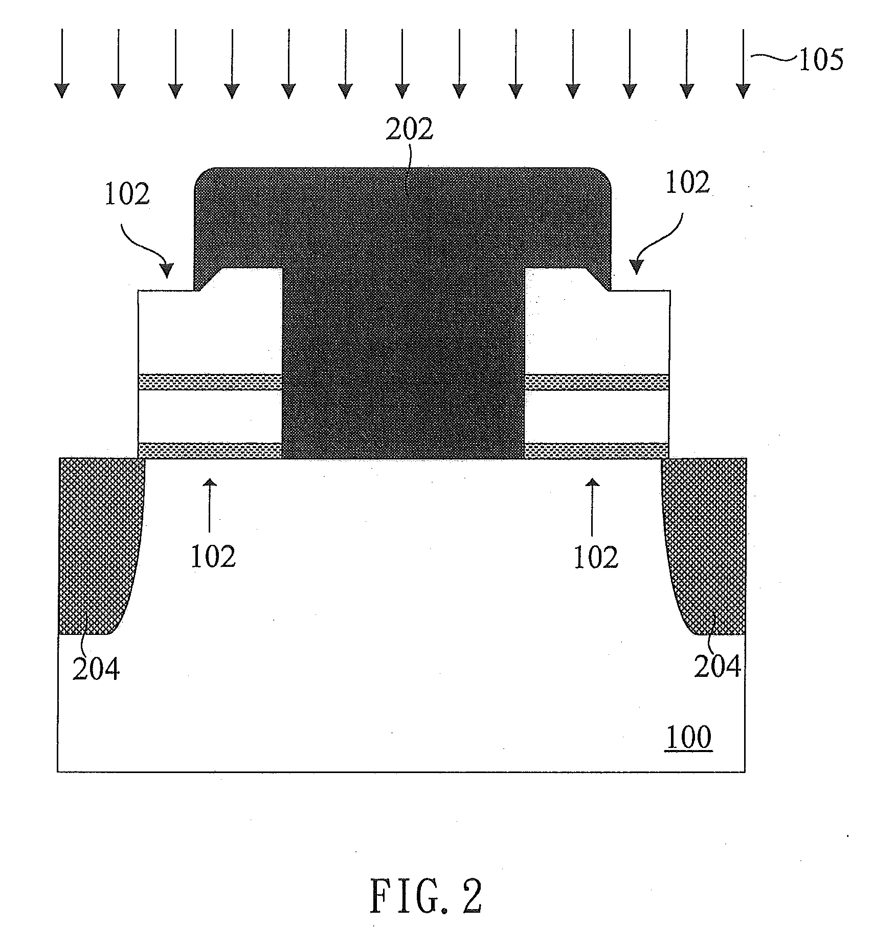
[0011]Please refer to FIGS. 1 to 9 that are schematic sectional views of a flash memory device at different stages in a method of manufacturing a flash memory device according to a preferred embodiment of the present invention. In FIG. 1, there is provided a semiconductor substrate 100, on which two gate structures 102 are formed. Each of the gate structures 102 includes a tunneling oxide layer 102a, a floating gate 102b, a dielectric layer 102c, and a control gate 102d. A channel 103 is also formed on the semiconductor substrate 100 between the two gate structures 102. The material for the semiconductor substrate 100 can be silicon, silicon-germanium (SiGe), silicon on insulator (SOI), silicon germanium on insulator (SGO...


PUM


Abstract

A flash memory device manufacturing process includes the steps of providing a semiconductor substrate; forming two gate structures on the substrate; performing an ion implantation process to form two first source regions in the substrate at two lateral outer sides of the two gate structures; performing a further ion implantation process to form a first drain region in the substrate between the two gate structures; performing a pocket implantation process between the gate structures to form two doped regions in the substrate at two opposite sides of the first drain region; forming two facing L-shaped spacer walls between the two gate structures above the first drain region; performing an ion implantation process to form a second drain region beneath the first drain region, both of which having a steep junction profile compared to the first source regions; and forming a barrier plug above the first drain region.

Description

FIELD OF THE INVENTION[0001]The present invention relates to a method of manufacturing a memory device, and more particularly to a method of manufacturing a flash memory device.BACKGROUND OF THE INVENTION[0002]With the progress in semiconductor process technique, the process technique for memory devices also moves into the era of nanometer technology. The reduction of device dimensions increases not only the density of integrated circuit (IC), but also the current driving ability of the device. However, the movement of the memory devices into the nanometer era also brings the problems of short channel effects (SCE) and gate leakage current. As a result, it becomes more difficult to enhance the memory device performance by reducing the channel length and gate oxide layer thickness of the memory device.[0003]For example, a lightly doped drain (LDD) enables the device to have an increased breakdown voltage, improved critical voltage property, and reduced hot carrier effect. While the l...

Claims


Application Information

Patent Timeline
IPC IPC(8): H01L21/8234
CPCH01L27/11519H01L21/28273H01L29/40114H10B41/10
Inventor CHEN, HUNG-WEIWU, YIDER
Owner EON SILICON SOLUTION
Learn More