Deep channel isolated drain metal-oxide-semiconductor transistors
- Summary
- Abstract
- Description
- Claims
- Application Information
AI Technical Summary
Benefits of technology
Problems solved by technology
Method used
Image
Examples
Embodiment Construction
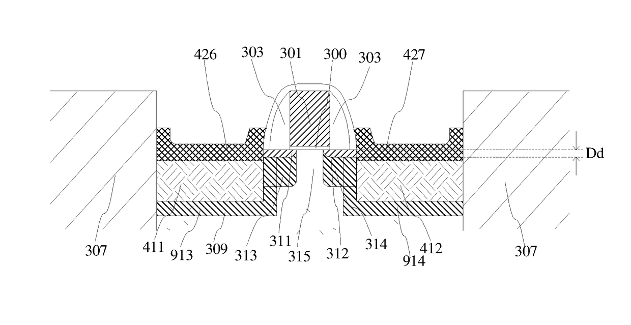
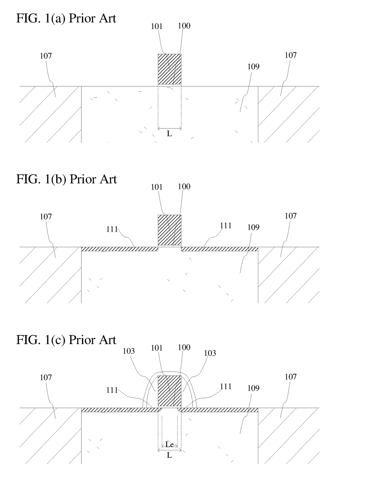
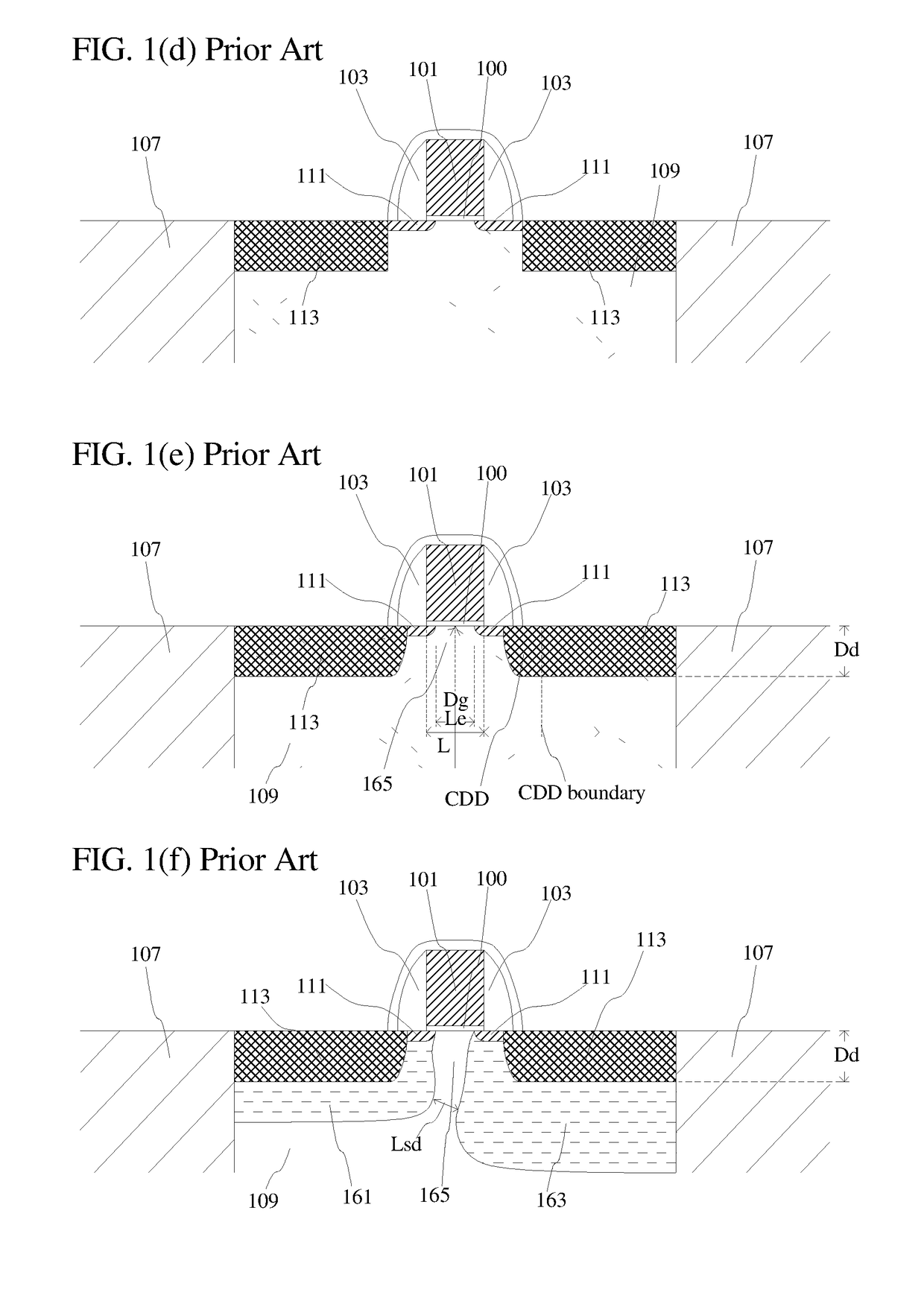
[0025]FIGS. 3(a-l) are symbolic cross-section diagrams illustrating exemplary manufacturing procedures for an MOS transistor of the present invention. FIG. 3(a) is a symbolic cross-section diagram that shows an active area of a semiconductor substrate (309) surrounded by field insulators (307). The semiconductor substrate (309) is etched to a depth about the same as the height of transistor gate stack, as shown in FIG. 3(b). In the following steps, gate insulator (300) and gate conductor (301) are formed on the semiconductor substrate (309), as shown in FIG. 3(c). After gate formation, a shallow drain diffusion region (311) and a barrier diffusion region (313) are implanted under the source-drain areas, as shown in FIG. 3(d). Using the gate conductor (301) and the field insulators (307) as masking materials, implantations of these two layers (311, 313) are self-aligned. For n-channel MOS transistors, the shallow drain diffusion region (311) is n-type, while the barrier diffusion reg...
PUM
 Abstract
Description
Claims
Application Information


