
Composite semiconductor device

a semiconductor device and semiconductor technology, applied in the direction of diodes, electronic switching, pulse techniques, etc., can solve the problem that the conventional gate drive circuit cannot be used

Active Publication Date: 2015-07-30
SHARP KK
View PDF1 Cites 1 Cited by
  • Summary
  • Abstract
  • Description
  • Claims
  • Application Information

AI Technical Summary

Benefits of technology

The composite semiconductor device described in this patent aims to prevent breakdown of a specific transistor without the need for an additional device that can cause unstable control. The device achieves this by keeping the drain voltage of another transistor lower than the breakdown voltage during a specific time period. However, this can only be achieved without using a specific process in the first place.

Problems solved by technology

If such a field effect transistor of normally on type is used in a semiconductor device, various problems such as that a conventional gate drive circuit cannot be used and the like occur.

Method used


Image

  • Composite semiconductor device
  • Composite semiconductor device
  • Composite semiconductor device

Examples


Embodiment Construction

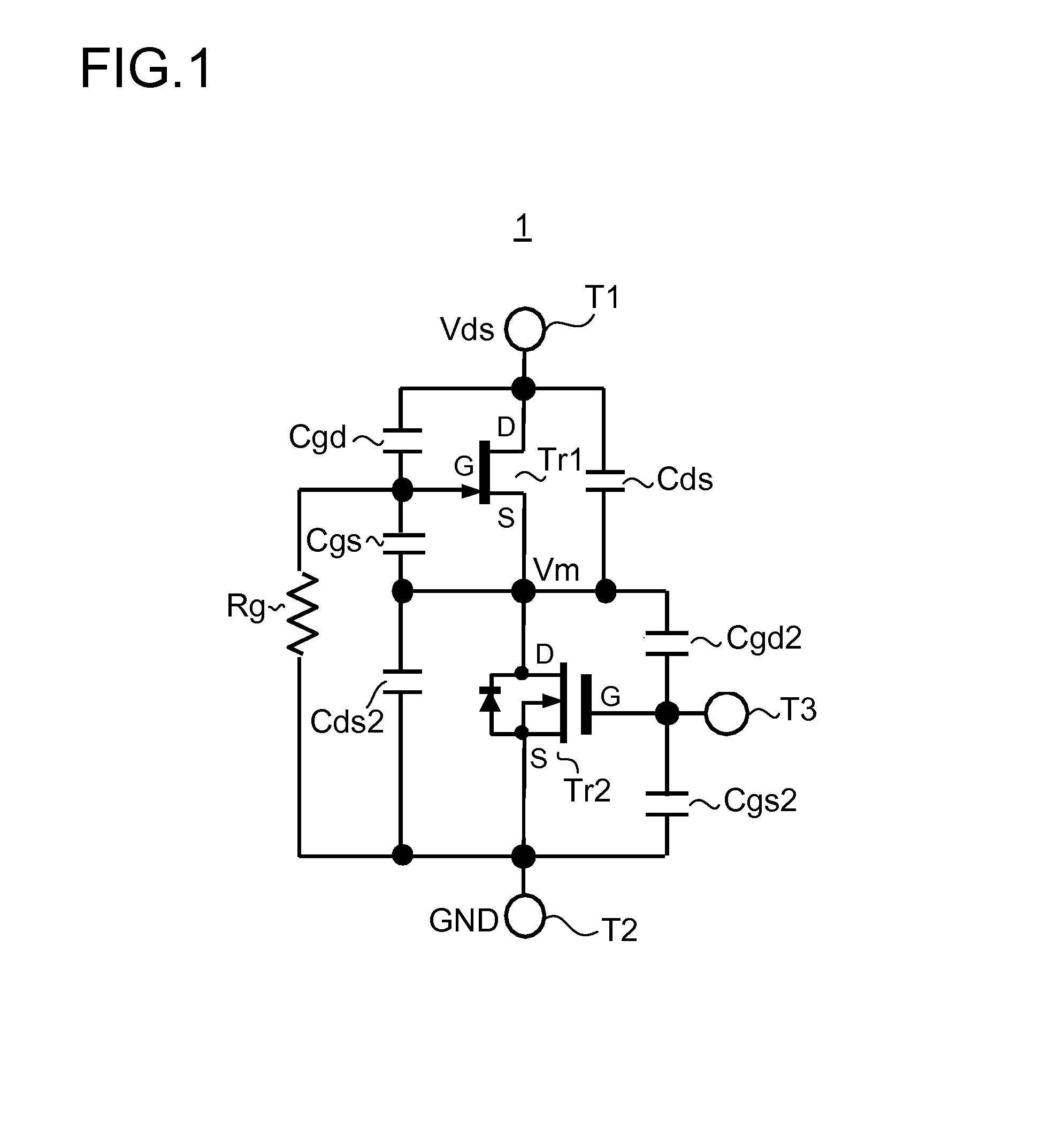
[0023]Hereinafter, an embodiment of the present invention is described with reference to the drawings. FIG. 1 shows a structure of a composite semiconductor device according to the embodiment of the present invention.

[0024]The composite semiconductor device 1 shown in FIG. 1 includes: a high-breakdown voltage first field effect transistor of normally on type (hereinafter, called a FET) Tr1; a low-breakdown voltage second FET Tr2 of normally off type; a gate-drain capacitance Cgd of the first FET Tr1; a gate-source capacitance Cgs of the first FET Tr1; a drain-source capacitance Cds of the first FET Tr1; a gate-drain capacitance Cgd2 of the second FET Tr2; a gate-source capacitance Cgs2 of the second FET Tr2; a drain-source capacitance Cds2 of the second FET Tr2; a gate resistance Rg; a power source terminal T1; a ground terminal T2; and a gate terminal T3.

[0025]The first FET Tr1 and the second FET Tr2 are connected in series with each other. The drain of the first FET Tr1 is connect...


PUM


Abstract

In a composite semiconductor device which is provided with a normally-on-type first transistor and a normally-off-type second transistor which are serially connected, the second transistor is selected so as to satisfy Formula (1):Coss>CdsVdsVbr-Cds-Cgs(1)In this regard: Coss: output capacitance of second transistor Cds: drain to source capacitance of first transistor Cgs: gate to source capacitance of first transistor Vds: power supply voltage Vbr: breakdown voltage of second transistor.

Description

TECHNICAL FIELD[0001]The present invention relates to a composite semiconductor device, more particularly, to a composite semiconductor device that includes a transistor of normally on type and a transistor of normally off type which are connected in series with each other.BACKGROUND ART[0002]Si(silicon)-based field effect transistors mainly used in semiconductor devices of today are of normally off type. A field effect transistor of normally off type is a transistor that is turned on in a case where a positive voltage is applied between a gate and a source, and turned off in a case where the positive voltage is not applied between the gate and the source.[0003]Besides, GaN (gallium nitride) based and SiC (silicon carbide)-based field effect transistors, whose practical use is under study because of features such as high breakdown voltage, low loss, high-speed switching, high-temperature operation and the like, are of normally on type. A transistor of normally on type has a negative...

Claims


Application Information

Patent Timeline
Patent Type & Authority Applications(United States)
IPC IPC(8): H01L27/06H01L27/088H01L49/02H10N97/00
CPCH01L27/0629H01L27/0883H01L28/20H03K17/102H03K2017/6875
Inventor OHSHIMA, YOSHIFUMI
Owner SHARP KK
Learn More