
Contact structure comprising semiconductor and metal islands

a contact structure and metal island technology, applied in semiconductor devices, semiconductor/solid-state device details, electrical apparatus, etc., can solve the problems of low work-function materials, high reactive materials, and certain approaches that have drawbacks, so as to reduce the barrier of charge carrier injection and improve the efficiency of carrier injection

Inactive Publication Date: 2010-02-09
INTERUNIVERSITAIR MICRO ELECTRONICS CENT (IMEC VZW)
View PDF15 Cites 1 Cited by
  • Summary
  • Abstract
  • Description
  • Claims
  • Application Information

AI Technical Summary

Benefits of technology

The granular metal contact structures enhance charge carrier injection efficiency by reducing injection barriers, enabling cost-effective production of devices with smaller geometries and improved performance by using a single contact material for both p-type and n-type semiconductor layers, while maintaining conductivity comparable to organic semiconductor materials.

Problems solved by technology

However, the use of different contact metals in OLEDs does not consistently provide for efficient charge injection into wide bandgap organic materials (e.g., materials with a bandgap>3 eV).
Such approaches have certain drawbacks, however.
For instance, such low work-function materials are highly reactive, which makes them difficult to process.
A further drawback is that such low work-function materials must be encapsulated in order to prevent degradation after removal from a vacuum environment in which they are processed (e.g., deposited, patterned, etc.).
Such precise positioning is an extremely difficult task for devices with channel lengths of a few micrometers or smaller.
Thus, such processes may experience significant yield loss due to alignment issues associated with such an approach.
Such yield loss would result in a corresponding increase in the cost of producing such devices.
Other limitations of the related art will become apparent to those of skill in the art upon a reading of the specification and a study of the drawings.

Method used


Image

  • Contact structure comprising semiconductor and metal islands
  • Contact structure comprising semiconductor and metal islands
  • Contact structure comprising semiconductor and metal islands

Examples


Embodiment Construction

Overview

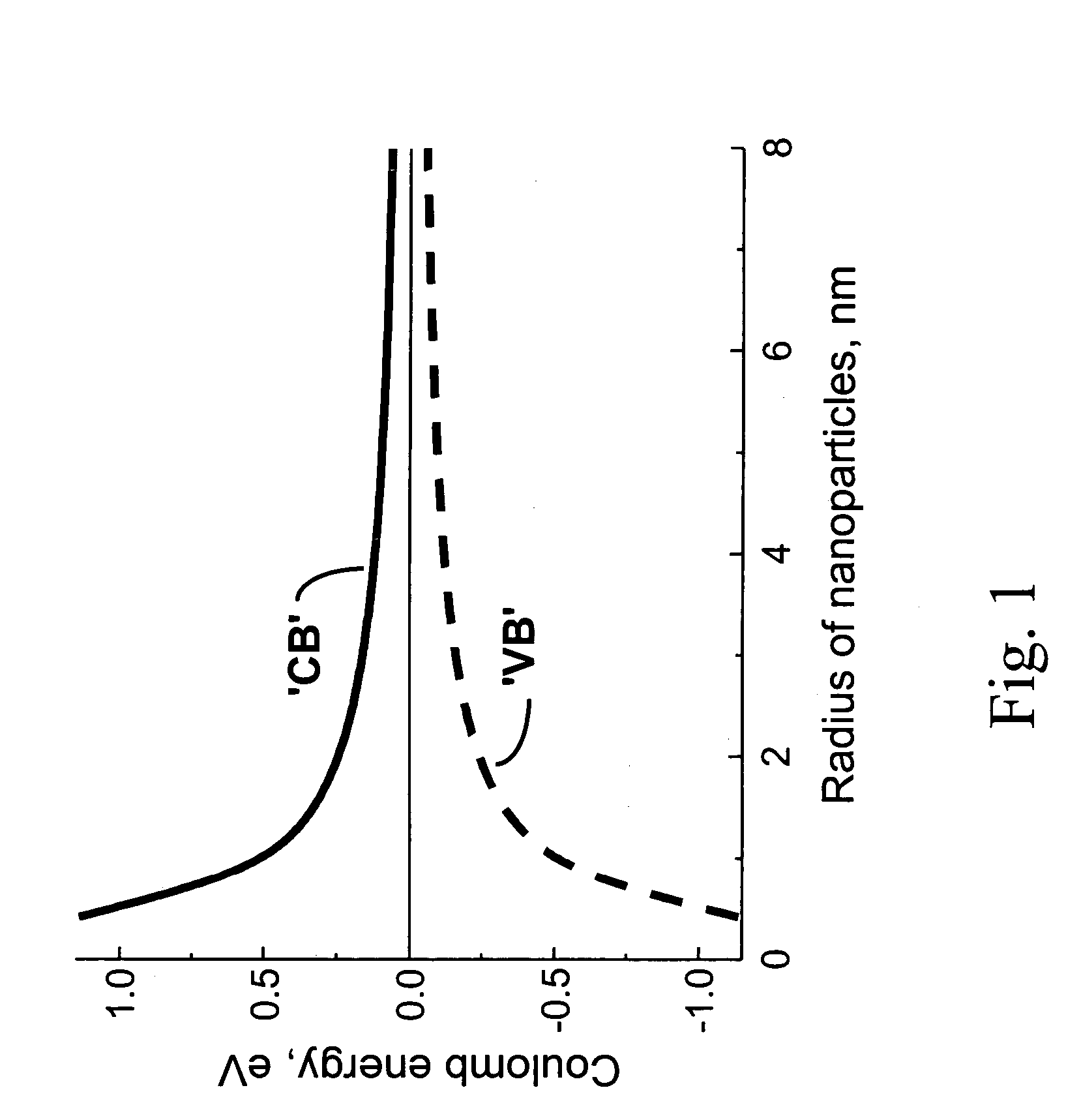
[0020]In order to overcome at least some of the drawbacks discussed above for electronic devices, such as, for example, complementary thin-film transistors (TFTs) using organic semiconductor materials or organic light-emitting thin-film transistors (OLETFTs), one potential solution would be to use a single contact deposition process to form the ohmic contacts (e.g., using the same contact material or materials) for both p-type and n-type semiconductor materials. Such an approach would be more cost effective than processes using two different contact materials as such an approach would reduce the number of masks steps required from, for example, two mask steps to a single mask step. Accordingly, such an approach would also reduce yield loss that results from the alignment precision issues described above. Furthermore, elimination of such alignment concerns would allow for the design and fabrication of devices with smaller critical geometries, such as channel lengths. Such des...


PUM

PropertyMeasurementUnit
electrostatic energyaaaaaaaaaa
distanceaaaaaaaaaa
distanceaaaaaaaaaa

Abstract

Contact structures and methods for forming such contact structures are disclosed. An example contact structure includes a layer of semiconductor material having an interface and an electrical contact at the interface of the layer of semiconductor material, where the electrical contact includes a granular metal. An example method for forming a contact structure includes providing a substrate and producing a granular metal on at least part of the substrate, where the granular metal includes a cluster of metal islands extending essentially in a two-dimensional plane. The method further includes depositing a layer of a semiconductor material on top of the substrate and the cluster of metal islands.

Description

CROSS REFERENCE TO RELATED APPLICATIONS[0001]This application claims benefit under 35 U.S.C. § 119 to U.S. Provisional Patent Application 60 / 601,192, filed Aug. 13, 2004 and of the same title as the present application. The entire disclosure of U.S. Provisional Patent Application 60 / 601,192 is incorporated herein by reference.BACKGROUND[0002]I. Field[0003]This disclosure relates to the field of microelectronics. More particularly, this disclosure relates to contacting structures for semiconductor materials and methods for fabrication of such structures.[0004]II. Description of Related Art[0005]Efficient and balanced injection of both electrons and holes is desirable in the operation of bipolar devices and / or electronic devices where complementary charge carriers are required, such as light-emitting diodes and complementary (e.g., n-type and p-type) transistors. In certain organic devices (e.g., organic light-emitting diodes (OLEDs)) this objective is achieved through the use of diff...

Claims


Application Information

Patent Timeline
Patent Type & Authority Patents(United States)
IPC IPC(8): H01L23/48
CPCH01L51/0021H01L51/5203Y02E10/549H10K71/60H10K50/805
Inventor ARKHIPOV, VLADIMIRHEREMANS, PAUL
Owner INTERUNIVERSITAIR MICRO ELECTRONICS CENT (IMEC VZW)
Learn More