
Semiconductor device and manufacturing method thereof

a technology of semiconductor devices and manufacturing methods, applied in the direction of semiconductor devices, electrical devices, transistors, etc., can solve the problems of difficult resistance mask formation, and achieve the effect of reducing the voltage of the signal to be applied to the control gate electrod

Inactive Publication Date: 2011-06-28
SEMICON ENERGY LAB CO LTD
View PDF32 Cites 2 Cited by
  • Summary
  • Abstract
  • Description
  • Claims
  • Application Information

AI Technical Summary

Benefits of technology

This approach ensures good retention properties, suppresses hot carrier deterioration, and achieves a semiconductor device with small variation and improved performance by maintaining equal overlap lengths and areas, while allowing for self-aligned control gate electrode formation without misalignment.

Problems solved by technology

However, it is difficult to form the resist mask 1008 properly at a desired position since a misalignment occurs depending on alignment precision of a device when the resist mask 1008 is formed.

Method used


Image

  • Semiconductor device and manufacturing method thereof
  • Semiconductor device and manufacturing method thereof
  • Semiconductor device and manufacturing method thereof

Examples


embodiment mode 1

[0070]A structure of a semiconductor device or the like is described here.

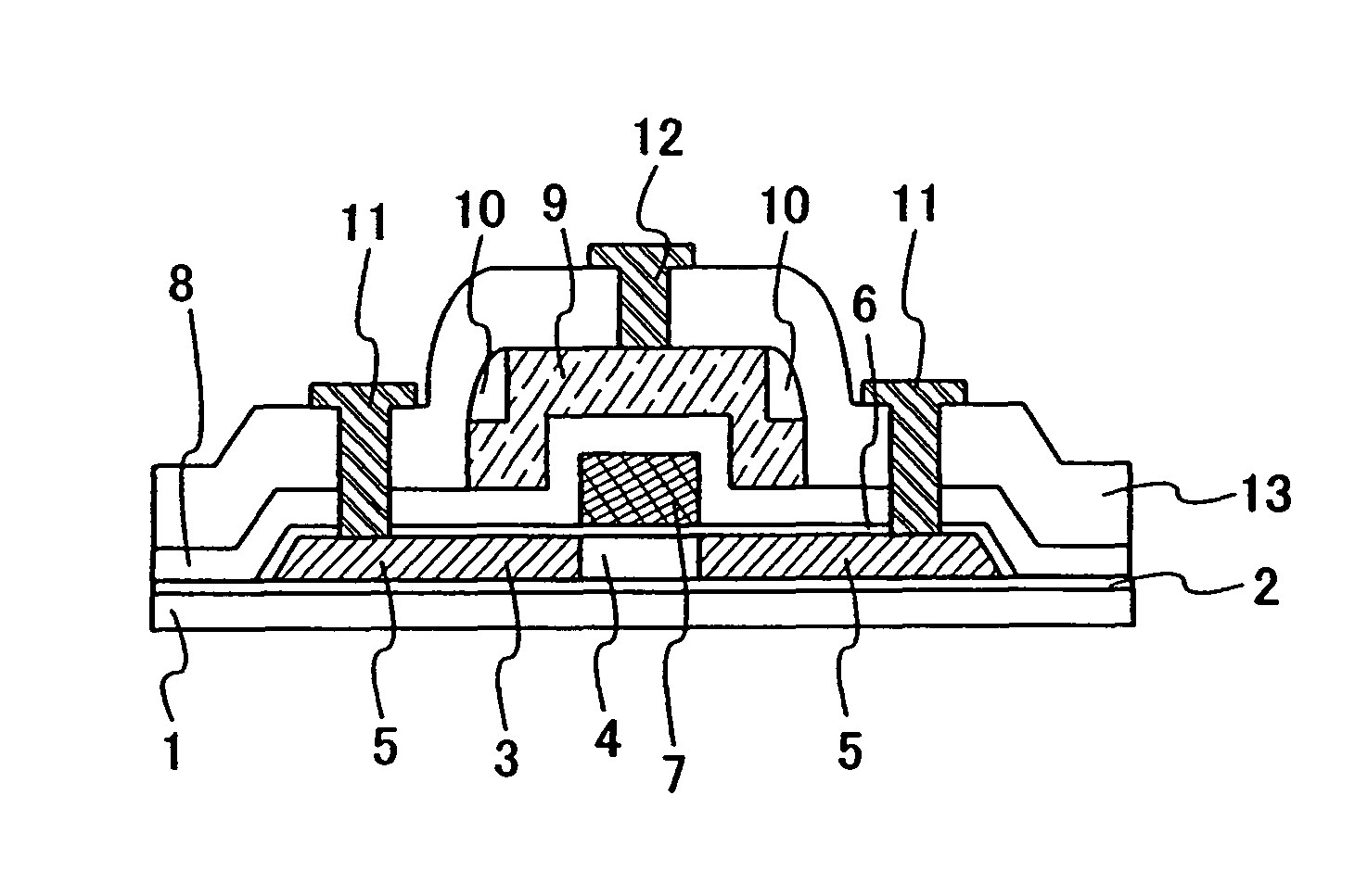
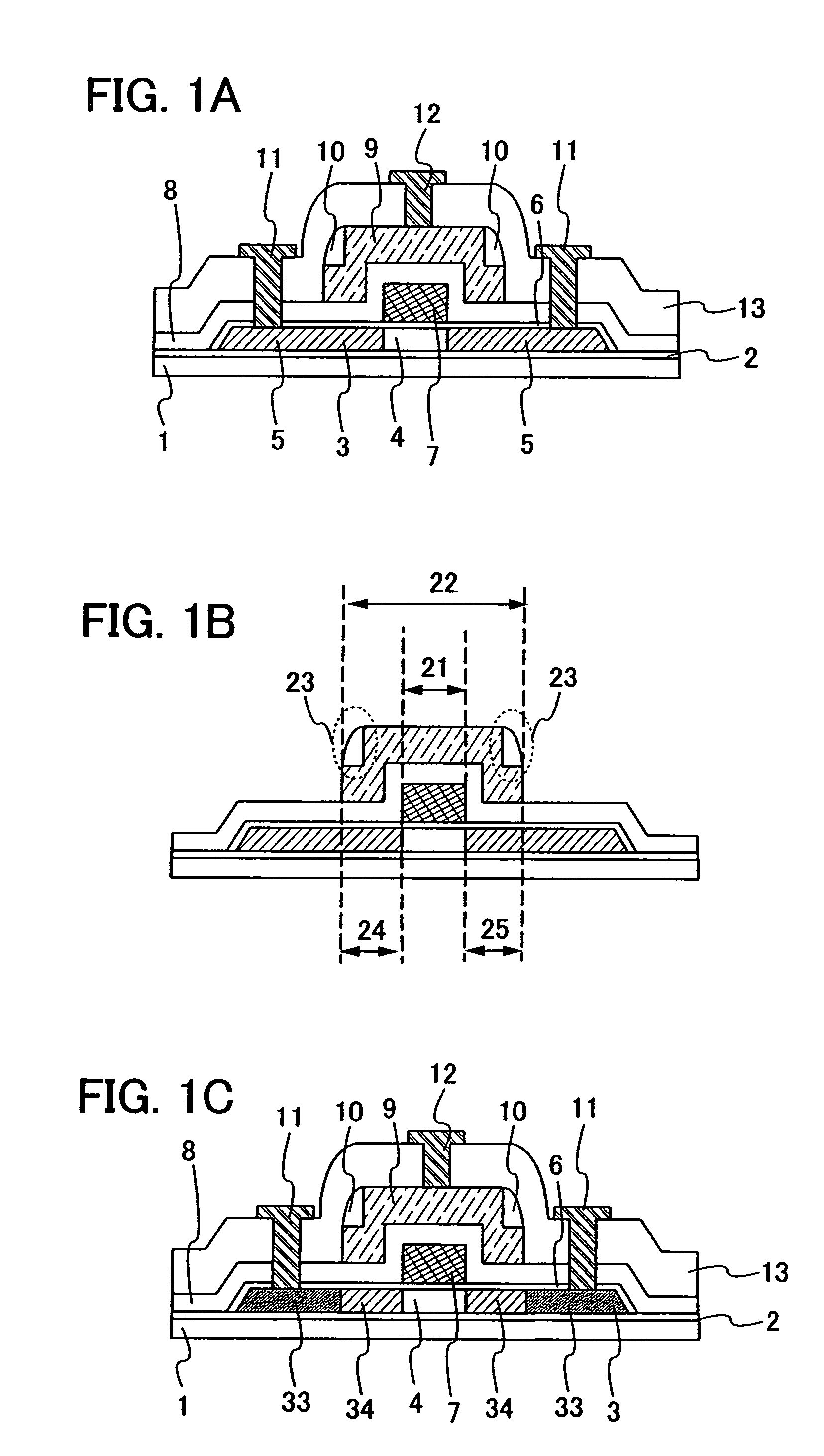
[0071]FIG. 1A is a schematic cross-sectional diagram showing an example of an embodiment mode of the present invention. Reference numeral 1 denotes a substrate, 2 denotes a base insulating film, 3 denotes a semiconductor film, 4 denotes a channel forming region, 5 denotes a source or drain region, 6 denotes a first gate insulating film (also called a tunnel insulating film), 7 denotes a floating gate electrode, 8 denotes a second gate insulating film (also called a control insulating film), 9 denotes a control gate electrode, 10 denotes a sidewall, 11 denotes a source or drain electrode electrically connected to the source or drain region 5, 12 denotes a gate wire electrically connected to the control gate electrode 9, and 13 denotes a passivation insulating film. The source or drain electrode 11, the gate wire 12, and the passivation insulating film 13 are formed if necessary.

[0072]In a structure shown in FIG...

embodiment mode 2

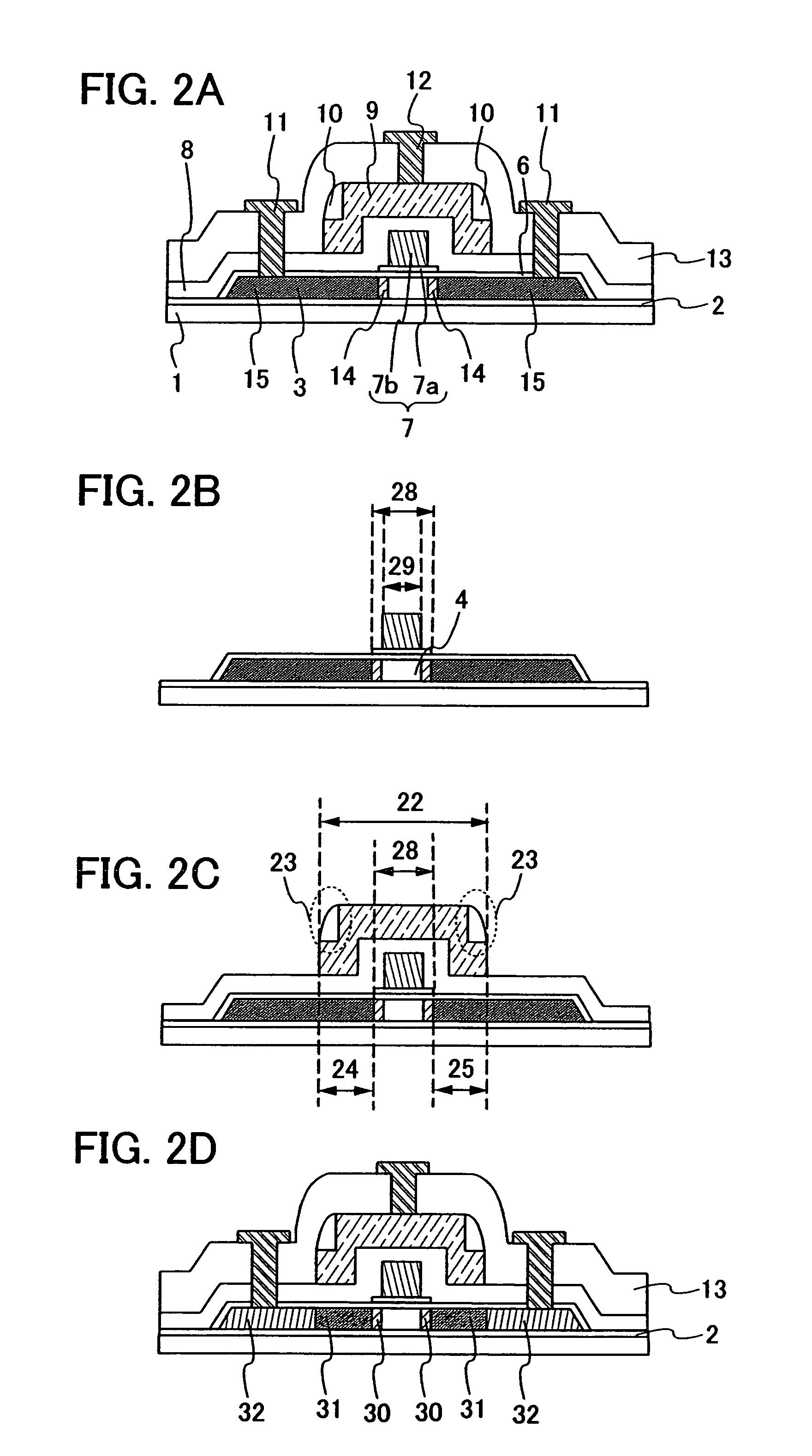
[0091]Here, a structure of a semiconductor device, or the like which is different from that of Embodiment Mode 1 is described. The differences from the semiconductor device of Embodiment Mode 1 are that first impurity regions 15, second impurity regions 14 and the like are provided in the semiconductor film 3, that the floating gate electrode 7 is structured by a first floating gate electrode 7a and a second floating gate electrode 7b, and the like.

[0092]FIG. 2A is a schematic cross-sectional diagram showing an example of another embodiment mode of the present invention. FIGS. 2B and 2C are a part of FIG. 2A. Note that the same portions are denoted by the same reference numerals as Embodiment Mode 1.

[0093]In FIG. 2A, reference numeral 7 denotes the floating gate electrode, 7a denotes the first floating gate electrode, 7b denotes the second floating gate electrode, 14 denotes the second impurity region, and 15 denotes the first impurity region.

[0094]In a structure shown in FIG. 2A, t...

embodiment mode 3

[0109]A method of manufacturing the semiconductor device described in Embodiment Mode 1, namely the semiconductor device shown in FIGS. 1A to 1C, is described here.

[0110]First, as shown in FIG. 4A, an insulating film 2 for preventing impurities or the like from diffusing from a substrate 1 side is formed with a thickness of 10 to 200 nm by using silicon oxide (SiOx), silicon nitride (SiNx), silicon oxynitride (SiOxNy) (x>y), silicon nitride oxide (SiNxOy) (x>y), or the like, over the substrate 1 having an insulating property such as a glass substrate or a plastic substrate.

[0111]Next, an amorphous silicon film is formed with a thickness of 40 to 100 nm by a CVD method as a semiconductor film 40. Since a crystalline silicon film 42 is used as the semiconductor film 3, the amorphous silicon film is crystallized here.

[0112]As a method of crystallizing the amorphous silicon film, there are a method of irradiating an amorphous silicon film with a laser beam 41 (FIG. 4B), a method of crys...


PUM


Abstract

A semiconductor device which is formed in a self-aligned manner without causing a problem of misalignment in forming a control gate electrode and in which a leak between the control gate electrode and a floating gate electrode is not generated, and a manufacturing method of the semiconductor device are provided. A semiconductor device includes a semiconductor film, a first gate insulating film over the semiconductor film, a floating gate electrode over the first gate insulating-film, a second gate insulating film which covers the floating gate electrode, and a control gate electrode over the second gate insulating film. The control gate electrode is formed so as to cover the floating gate electrode with the second gate insulating film interposed therebetween, the control gate electrode is provided with a sidewall, and the sidewall is formed on a stepped portion of the control gate-electrode, generated due to the floating gate electrode.

Description

BACKGROUND OF THE INVENTION[0001]1. Field of the Invention[0002]The present invention relates to a technique relating to a semiconductor device formed over a substrate.[0003]2. Description of the Related Art[0004]At present, semiconductor memory devices for a personal computer, a digital camera, a mobile phone device, a household electrical appliance, an RFID, and the like have been actively developed. In particular, various configurations and structures have been researched and developed mainly on an EEPROM, and a flash memory each having a floating gate structure. Techniques in which a semiconductor memory device is formed not only over a silicon wafer but over a glass substrate, a plastic substrate, and a silicon wafer including an insulating layer have also been developed. Such a semiconductor memory device is disclosed, for example, in Reference 1 (Japanese Published Patent Application No. Hei 5-82787) and the like. A structure of a semiconductor memory device disclosed in Refe...

Claims


Application Information

Patent Timeline
Patent Type & Authority Patents(United States)
IPC IPC(8): H01L29/788H01L29/66H10B69/00
CPCH01L21/28273H01L21/84H01L27/115H01L27/11526H01L27/11546H01L27/13H01L29/66825H01L29/78621H01L27/12H01L2029/7863H01L27/1214H01L27/1266H01L29/40114H01L27/1255H10B41/49H10B41/40H10B69/00H01L21/31144
Inventor ASAMI, YOSHINOBU
Owner SEMICON ENERGY LAB CO LTD
Learn More