Method of manufacturing a plasma display panel

a technology of plasma display panel and manufacturing method, which is applied in the manufacture of electric discharge tubes/lamps, cold cathode manufacturing, and the manufacture of electromechanical systems, etc., can solve the problems of reducing the use efficiency of material layers, reducing the number of steps needed for forming ribs, and remarkably increasing the production cost of ribs

Inactive Publication Date: 2005-11-03
FUJITSU HITACHI PLASMA DISPLAY LTD
View PDF8 Cites 0 Cited by
  • Summary
  • Abstract
  • Description
  • Claims
  • Application Information

AI Technical Summary

Benefits of technology

[0010] The present invention has been achieved to solve the above problems. An object of the present invention is to provide a method of manufacturing a PDP in which a dielectric layer covering the entire surface of a substrate need not be provided, thermal oxidation of terminals is not caused by firing of a rib paste (green rib), no gaps are formed at an interface between each electrode and the a rib paste during the firing of the rib paste, and a portion of a terminal protective layer can be etched away by use of acid such as nitric acid.
[0011] The present invention provides a method of manufacturing a panel assembly for a PDP having electrodes and ribs formed on a substrate. The method comprises forming the electrodes on the substrate so that these electrodes are extended to a periphery of the substrate to form their terminals; applying a terminal protective paste on the terminals for protecting the terminals; applying a rib paste on the entire area of a rib formation region provided on the substrate to form a rib paste layer; molding the rib paste layer by use of a stamping die having cavities in the form of rib shape into green ribs; and firing the terminal protective paste and green ribs simultaneously to form a terminal protective layer and ribs on the substrate. Accordingly, after at least the terminals of electrodes are covered by applying the terminal protective paste thereon and a display region (also referred to as the rib formation region) is fully covered by applying the rib paste thereon, in short, after the electrodes and terminals are evenly covered with the terminal protective paste and rib paste, both of the pastes are fired simultaneously. Thus, the terminal protective paste covers portions of the electrodes which are not covered with the rib paste, and that is, both of the rib paste and terminal protective paste cover all the portions of the electrodes. Therefore, the electrodes and terminals can be sintered without causing thermal oxidization thereof while the rib paste and a phosphor paste are fired and the periphery of panel assemblies is sealed. Also, the time required for forming the terminal protective paste and rib paste can be reduced.

Problems solved by technology

However, a great number of steps are needed for forming the ribs by the sandblasting method as described above.
In addition, the rib material layer thus formed is cut and discarded by more than half, so that use efficiency of the material layer is decreased and rib production costs are remarkably increased.
This measure, however, has a disadvantage that adhesion of the rib paste to the electrodes is not good.
That is, because a firing temperature of the rib paste (green rib) is equal to or less than a softening temperature of glass contained in the rib paste, and for this reason, even if the rib paste (green rib) is fired, a glass material contained in the rib paste does not melt enough to flow liquidly, so that a gap is liable to occur at an interface between the electrodes and the rib paste.
Thus, there is a problem that a leak (of discharge gas) may be caused by the gap at a periphery portion of panel assemblies sealed with the sealing material.
However, since the rib paste contains a large amount of filler such as an alumina filler, the paste is hardly dissolved in acid such as nitric acid and it is difficult to etch away the portion of the terminal protective layer, which is problematic for the conventional PDP.

Method used


Image

  • Method of manufacturing a plasma display panel
  • Method of manufacturing a plasma display panel
  • Method of manufacturing a plasma display panel

Examples


first embodiment

the Present Invention

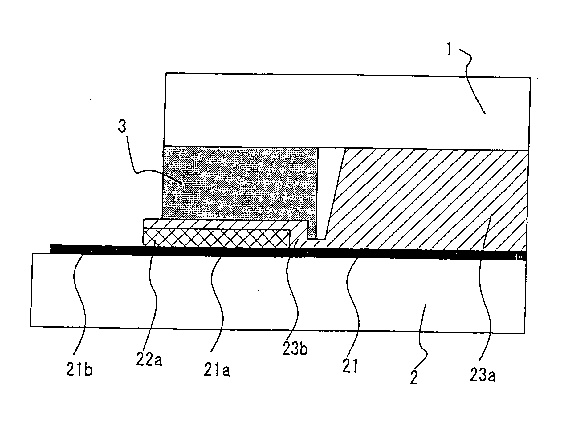
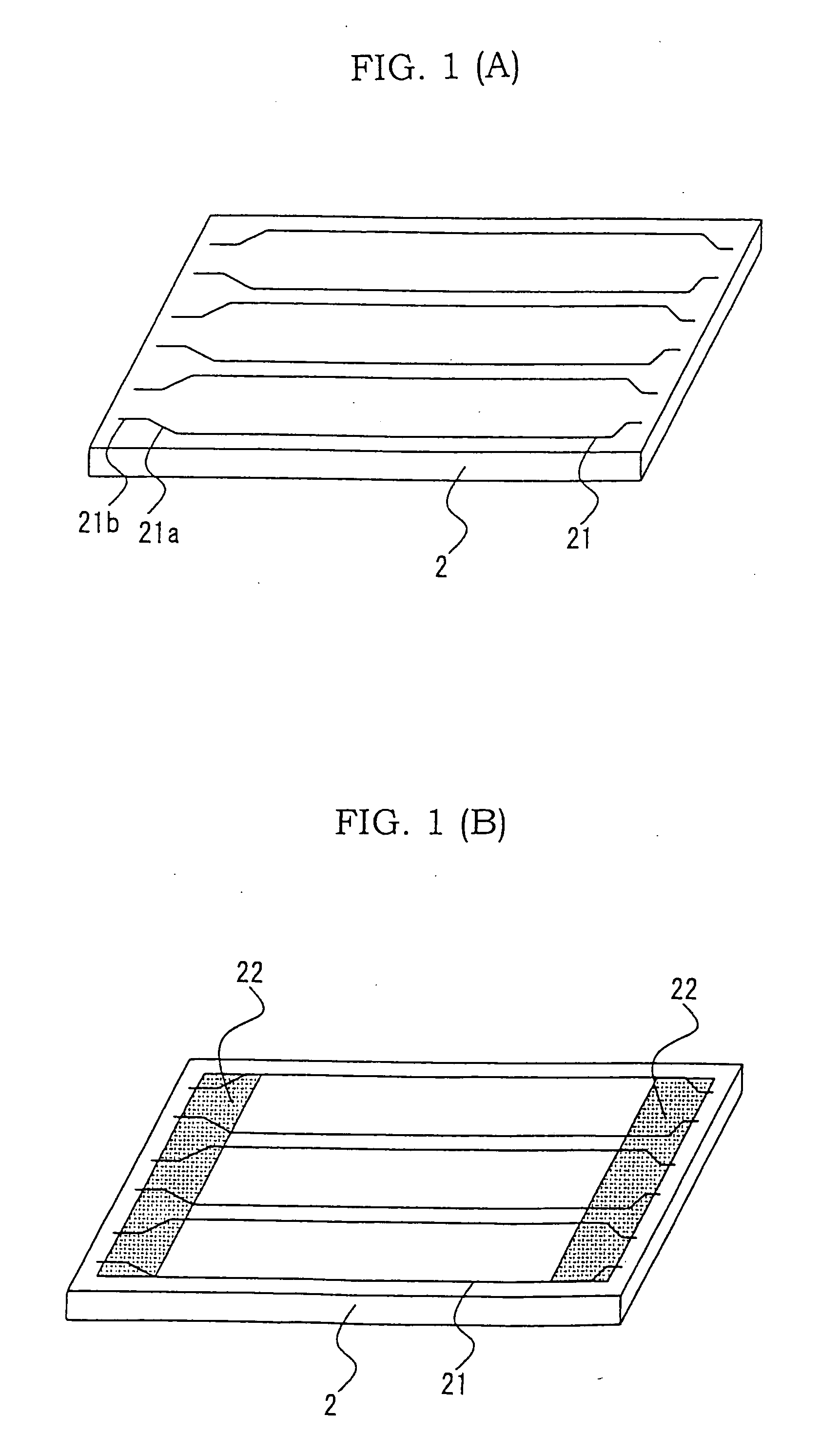
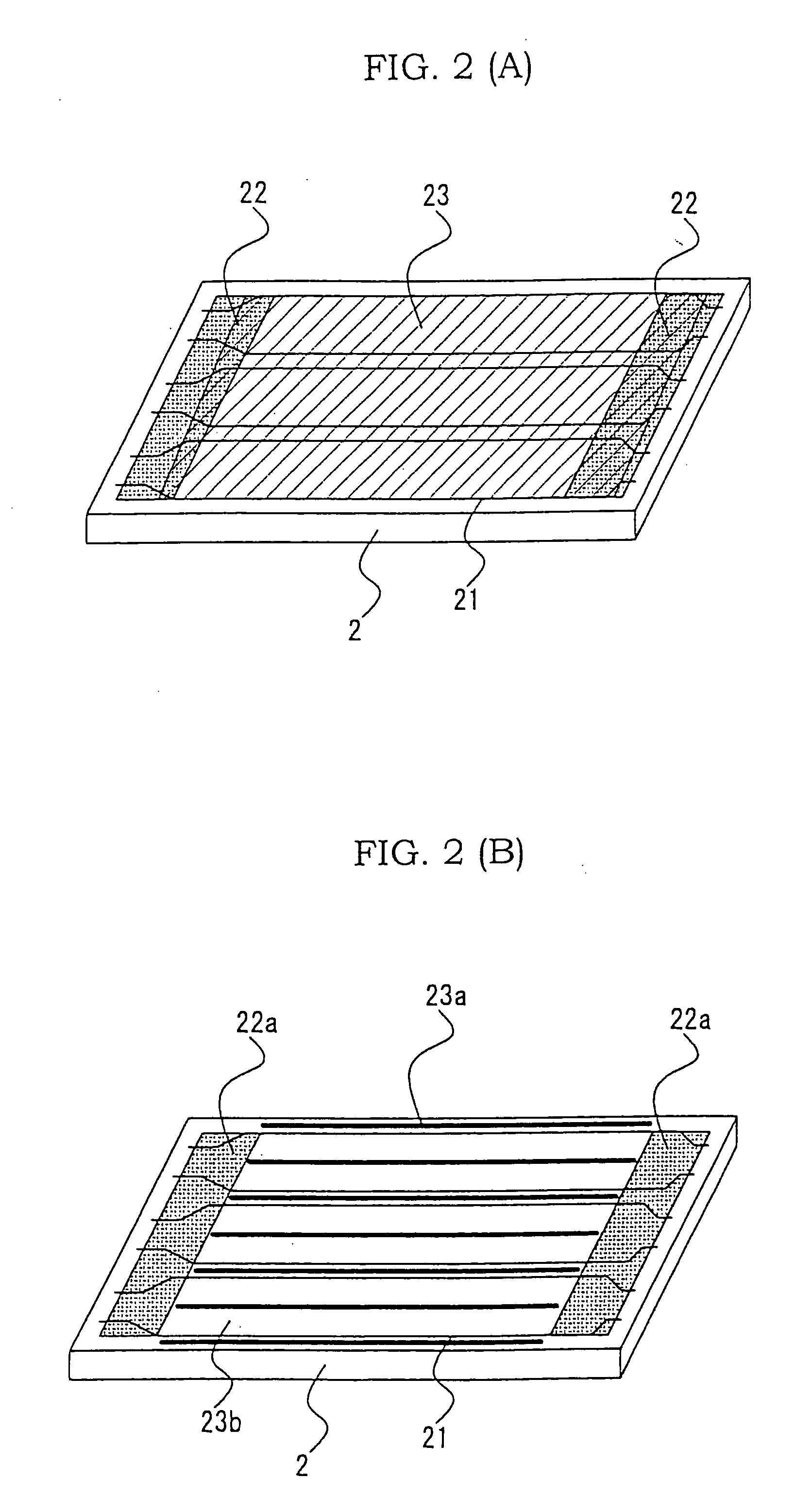
[0025] A method of manufacturing a PDP according to a first embodiment of the present invention is explained referring to FIGS. 1-4. FIGS. 1-3 are views for showing the state of a substrate with ribs after the steps of manufacturing the PDP according to the first embodiment. FIG. 4(A) illustrates a top view of an essential portion of the PDP according to the first embodiment and FIG. 4(B) illustrates a sectional view of the essential portion of the PDP according to the first embodiment.

[0026] The method of manufacturing the PDP of the first embodiment can be roughly divided into two processes. One process is to form a front panel assembly of the PDP. The other process is to form a rear panel assembly having ribs thereof. Here, explanation of the process of forming the front panel assembly is omitted since the front panel assembly can be formed by a typical technique and the process of forming the rear panel assembly will be described below.

[0027] The rear pane...

second embodiment

the Present Invention

[0036] A method of manufacturing a PDP according to a second embodiment of the present invention will be explained below. The PDP manufacturing method of the present invention is based on the premise that a molding process is employed. The molding process presents the following problem of the rib formation. Where the rib formation is performed by the molding process according to an ordinary method of manufacturing the PDP, edge portions of the rib paste 23 are spread when the rib paste 23 is patterned into a predetermined shape by pressing the thin plate elastic mold against the paste 23. For this reason, the rib paste 23 spreads to the outside of an appropriate region where ribs are to be formed. Specifically, it may spread over the lead portion 2b (see FIG. 4(A)) to the terminal portion 2c. Consequently, the rear substrate 2 at the terminal portion 2c is provided with a two-layer structure constituted of the terminal protective paste 22 and rib paste 23 and wh...

third embodiment

the Present Invention

[0042] A PDP manufacturing method according to a third embodiment of the present invention is performed in substantially the same manner as in the first and second embodiments, except that a photo-cure organic binder is used as an organic binder for the terminal protective paste 22 and the protective paste 22 is cured by the irradiation of light.

[0043] When the thermosetting organic binder is used as the organic binder, the terminal protective paste needs to be dried after it is applied. In general, the drying is performed by heating the substrate up to a temperature of approximately 100-200° C., but this substrate temperature needs to be lowered after the drying. If the formation of ribs is performed without lowering the substrate temperature, the substrate will be shrunk at about 7 ppm / ° C. and the accuracy of the ribs will be deteriorated. For these reasons, the lowering of substrate temperature is performed in order to keep the accuracy of the rib formation...


PUM


Abstract

A method of manufacturing a panel assembly is used for making a plasma display panel having electrodes and ribs formed on a substrate. The method includes the steps of forming the electrodes on the substrate so that these electrodes are extended to a periphery of the substrate to form their terminals, applying a terminal protective paste on the terminals for protecting the terminals, applying a rib paste on the entire area of a rib formation region provided on the substrate, molding the rib paste by use of a stamping die having cavities in the form of rib shape into green ribs, and firing the terminal protective paste and the green ribs simultaneously to form a terminal protective layer and ribs on the substrate.

Description

CROSS-REFERENCE TO RELATED APPLICATION [0001] This application is related to Japanese Patent Application No. 2002-255100 filed on Aug. 30, 2002, whose priority is claimed under 35 USC § 119, the disclosure of which is incorporated by reference in its entirety. BACKGROUND OF THE INVENTION [0002] 1. Field of the Invention [0003] The present invention relates to a method of manufacturing a plasma display panel, and more particularly to a method of manufacturing a substrate with ribs for a plasma display panel. [0004] 2. Description of the Related Art [0005] In general, ribs (also referred to as “barrier ribs”) for partitioning a discharge space of a conventional plasma display panel (hereinafter, PDP) are formed by a sandblasting method. The sandblasting method is performed as follows. On a substrate (for example, a rear substrate) on which electrodes and a dielectric layer to cover the electrodes for protecting them from the sandblasting are formed, a rib paste is applied to have a pr...

Claims


Application Information

Patent Timeline
Patent Type & Authority Applications(United States)
IPC IPC(8): H01J9/02H01J9/32H01J11/22H01J11/34H01J11/36H01J11/38H01J11/46
CPCH01J9/02H01J9/323H01J11/46H01J11/36H01J11/12H01J11/40
Inventor OHKUBO, TATSUYASHIRAKAWA, YOSHIMI
Owner FUJITSU HITACHI PLASMA DISPLAY LTD
Why Eureka
Try Eureka