

Method and device for detecting patterns on a substrate
a technology of pattern detection and substrate, applied in the direction of electromagnetic radiation sensing, semiconductor/solid-state device testing/measurement, instruments, etc., can solve the problems of one holographic pattern stepping over a connection, eccentric application of hologram, and inability to allow a small shi
- Summary
- Abstract
- Description
- Claims
- Application Information
AI Technical Summary
Benefits of technology
Problems solved by technology
Method used
Image

Examples
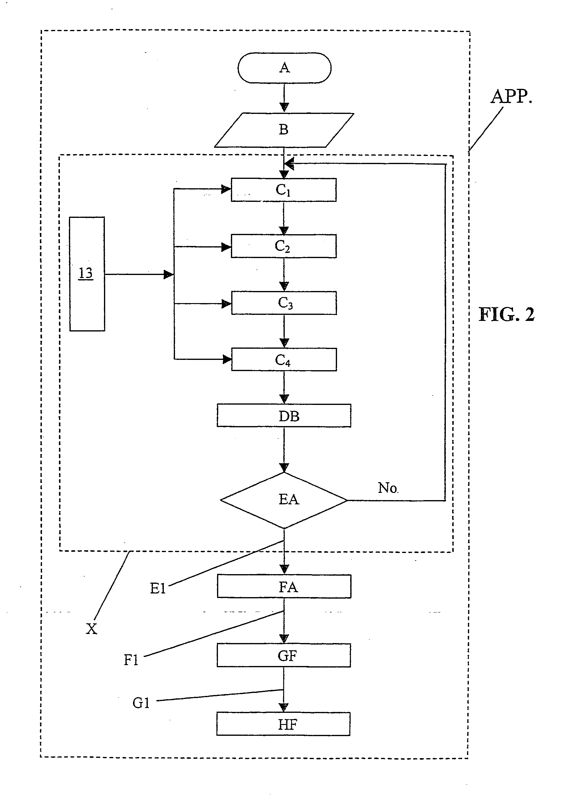
Embodiment Construction
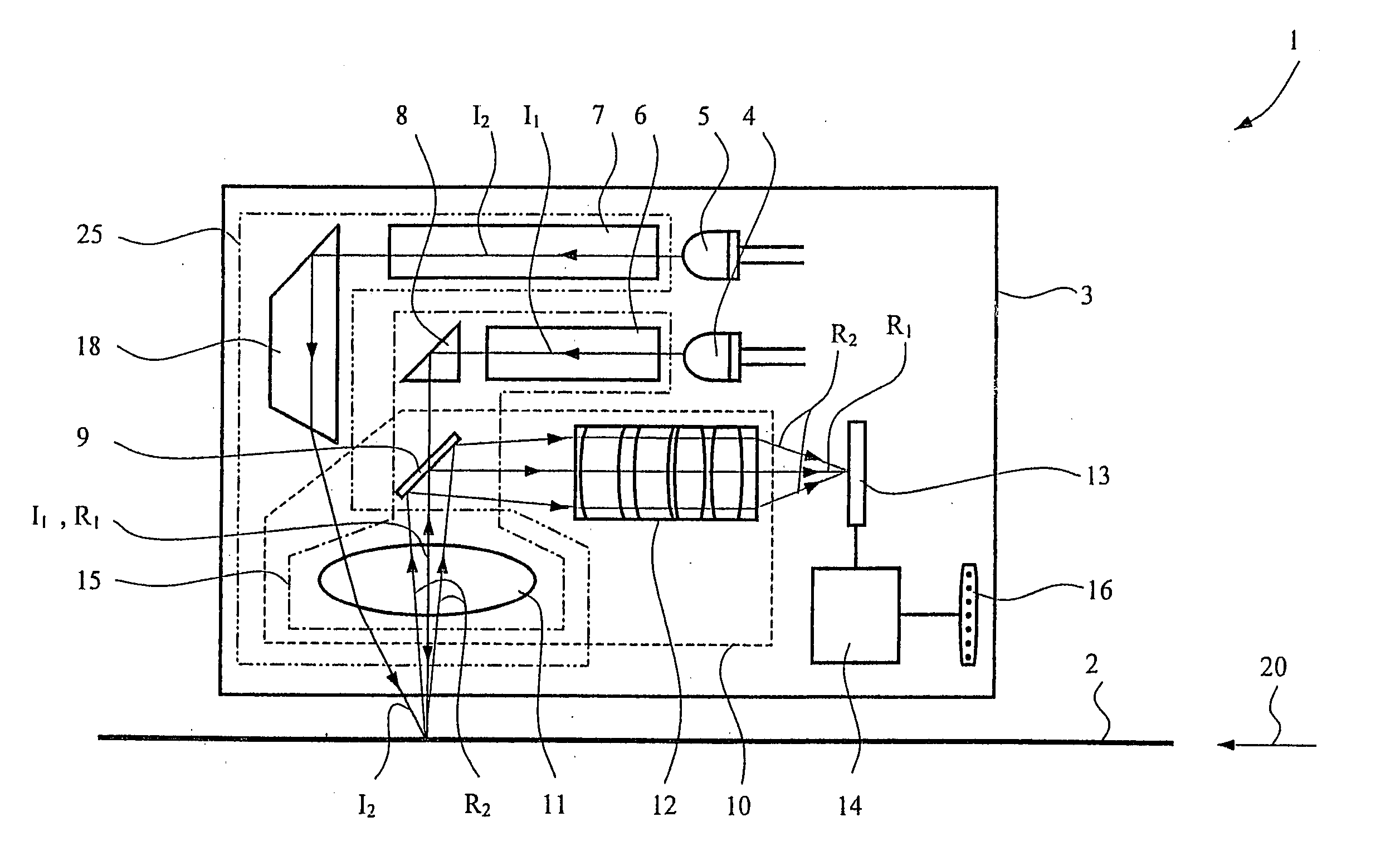
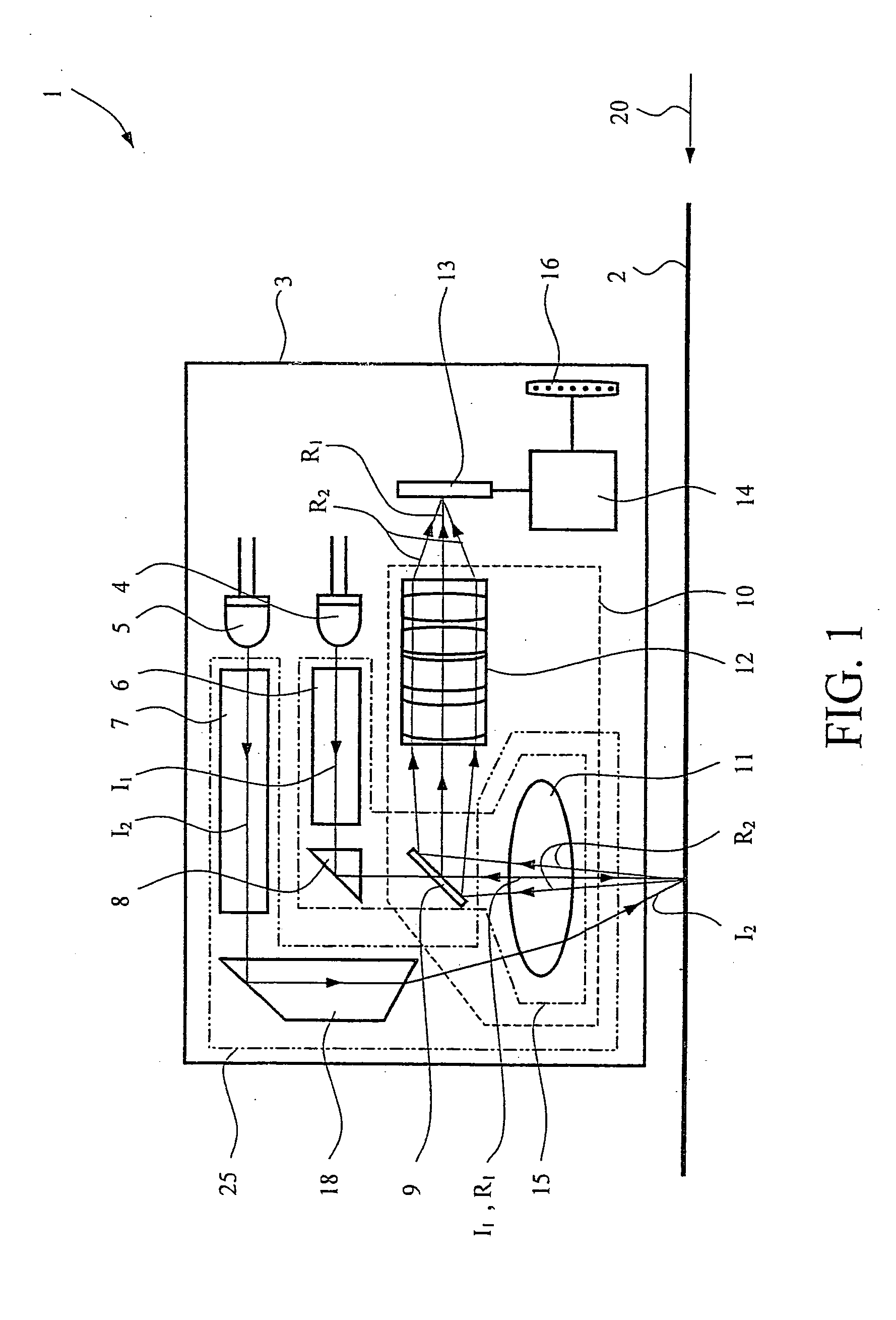
[0023]FIG. 1 is a schematic view of the device 1 for detecting patterns on a travelling substrate 2, being deposited on a foil or sheet matter, wherein the substrate travels through a driving means in a travelling direction 20 illustrated by a corresponding arrow. The detection device 1 is enclosed in a housing 3. The device comprises at least a first source of light 4 and a second source of light 5, each source possibly generating a light of at least two colors, preferably a first color like blue and a second color like red. The color choice is preferably based on colors being relatively spaced the one another in the visible spectrum, in order to improve the measuring result and more particularly to increase the contrast of the delivered image. The sources of light 4, 5 each emit a first incidental beam I1 and a second incidental beam I2. Each beam respectively enters a first and a second optical unit 6, 7 which may be a homogenizer, a mixer or a light condenser, even more than one...
PUM
| Property | Measurement | Unit |
|---|---|---|
| semi-transparent | aaaaa | aaaaa |
| angle of incidence | aaaaa | aaaaa |
| semi transparent | aaaaa | aaaaa |
Abstract
Description
Claims
Application Information