Passive optical sensor using carbon nanotubes

a carbon nanotube and optical sensor technology, applied in the field of passive optical sensors, can solve the problems of optical interconnections that demonstrate dramatic variation in amplitude loss, the information encoding method that sends information regarding the value being measured in the form of amplitude modulation of light signals is not desired, and the requirements of no other technology have been able to demonstrate a potential, etc., to achieve the effect of modulating the fermi level in the nanotube and dramatic effect on nanotubes

Inactive Publication Date: 2005-11-10
PETTIT JOHN W
View PDF4 Cites 7 Cited by
  • Summary
  • Abstract
  • Description
  • Claims
  • Application Information

AI Technical Summary

Benefits of technology

[0019] With regard to the first technique mentioned above, it has been reviewed in the research literature that carbon nanotubes exhibit a phemonenon where their bandgap changes upon physical distortion, such as twisting or elongation or radial compression [References 7 through 10]. This effect is related to further stressing of the sp2 hybrid bonds as described above, in a simplified view of the effect of the physical distortion on the nanotube band structure. It has been shown that, in the case of a compressive radial distortion that has the effect of flattening the nanotube, a radial compression of about 22% for certain nanotubes causes the bandgap to completely close. The nanotube has then undergone a semiconductor to metallic transition. It was then shown that further distortion opened up the bandgap again, making for a metallic to semiconducting transition.
[0020] When a nanotube demonstrates an optical transition between, for instance, the first van Hove singularity in the valence band to the first van Hove singularity in the conduction band, this manifests itself as a narrow bandwidth absorption resonance in the optical transmission spectrum of the nanotube. The present inventor was the first to recognize, to his knowledge, that changing the nanotube bandgap also changes the distance between these two van Hove singularities and consequently changes the wavelength of the optical absorption of the nanotube. When the bandgap changes, so does the distance between the two van Hove singularities and the wavelength at which the optical absorption resonance changes accordingly. The only reference that marginally suggests this effect is Reference 5, where the optical spectra of nanotubes in micelles, or floating in surfactant solution was different from the optical spectra of nanotubes deposited onto a flat substrate. It was theorized by Axel Hagen and Tobias Hertel that the stresses on the nanotube were caused by imperfections in the substrate surface as the nanotube cling to the surface through van der Walls forces. This caused distortions in the nanotubes that may have altered the bandgap, but they did not actually say this in their research report [Reference 5]. Axel Hagen and Tobias Hertel estimated that this casued a blue shift in the nanotube spectra of about 65 nanomteres and this seemed to be consistent with the published values of nanotube compressive modulus and the amount of strain that could reasonably be estimated from the surface imperfections.
[0021] The second technique is based on selective modulation of nanotube optical absorption. The Fermi level is the level to which electrons actually populate the allowed states in any given nanotube [Reference 6]. The Fermi level typically sits somewhere near the center of the bandgap in semiconducting nanotubes. Electrons can be either supplied to or taken away from the population of electrons in a nanotube by action of electric fields that are very near the nanotubes surface [References 2 through 4]. This has the effect of modulating the Fermi level in the nanotube. The phenomenon for this mechanism is called charge transfer doping and the electric field acts through what has been termed the “quantum capacitance” or sometimes the “chemical capacitance”. This is another remarkable feature of carbon nanotubes. Electric fields acting very near the surface have a dramatic effect on nanotubes, so much so that single molecule sensors have been proposed based on this phenomenon. On the other hand externally generated electric fields have almost no effect on nanotubes [References 1-2] up to hundreds of millions of volts per meter. This gives the nanotubes the essential property of immunity from large amounts of EMI, which is a critical need for the Air Force.

Problems solved by technology

These are a very challenging set of requirements that no other technology has been able to demonstrate a potential to meet.
In particular, information encoding methods that send information regarding the value that is being measured in the form of amplitude modulation of the light signal are not desired.
This is mostly due to the fact that optical interconnections demonstrate dramatically variable amplitude losses.
This gives rise to the need to recalibrate the system every time an optical connection is remade or when shock, vibration or strain changes the optical loss of a fiber optic connector.
Such a recalibration requirement is unworkable in practice and is therefore unacceptable.
This general technique has the problem that the light path through the optical network has to remain steady in that light losses cannot vary over time or through any other effects.
This condition is almost never met in practical fiber optic networks, especially networks that operate on aircraft.
This makes sensors that utilize light amplitude as their means of transmitting information not acceptable for this application.
However, the properties of carbon nanotubes noted above have not yet been exploited in a passive optical sensor which can meet the above-noted requirements.

Method used


Image

  • Passive optical sensor using carbon nanotubes
  • Passive optical sensor using carbon nanotubes
  • Passive optical sensor using carbon nanotubes

Examples


Embodiment Construction

[0043] Two preferred embodiments of the present invention will be set forth in detail with reference to the drawings, in which like reference numerals refer to like elements throughout.

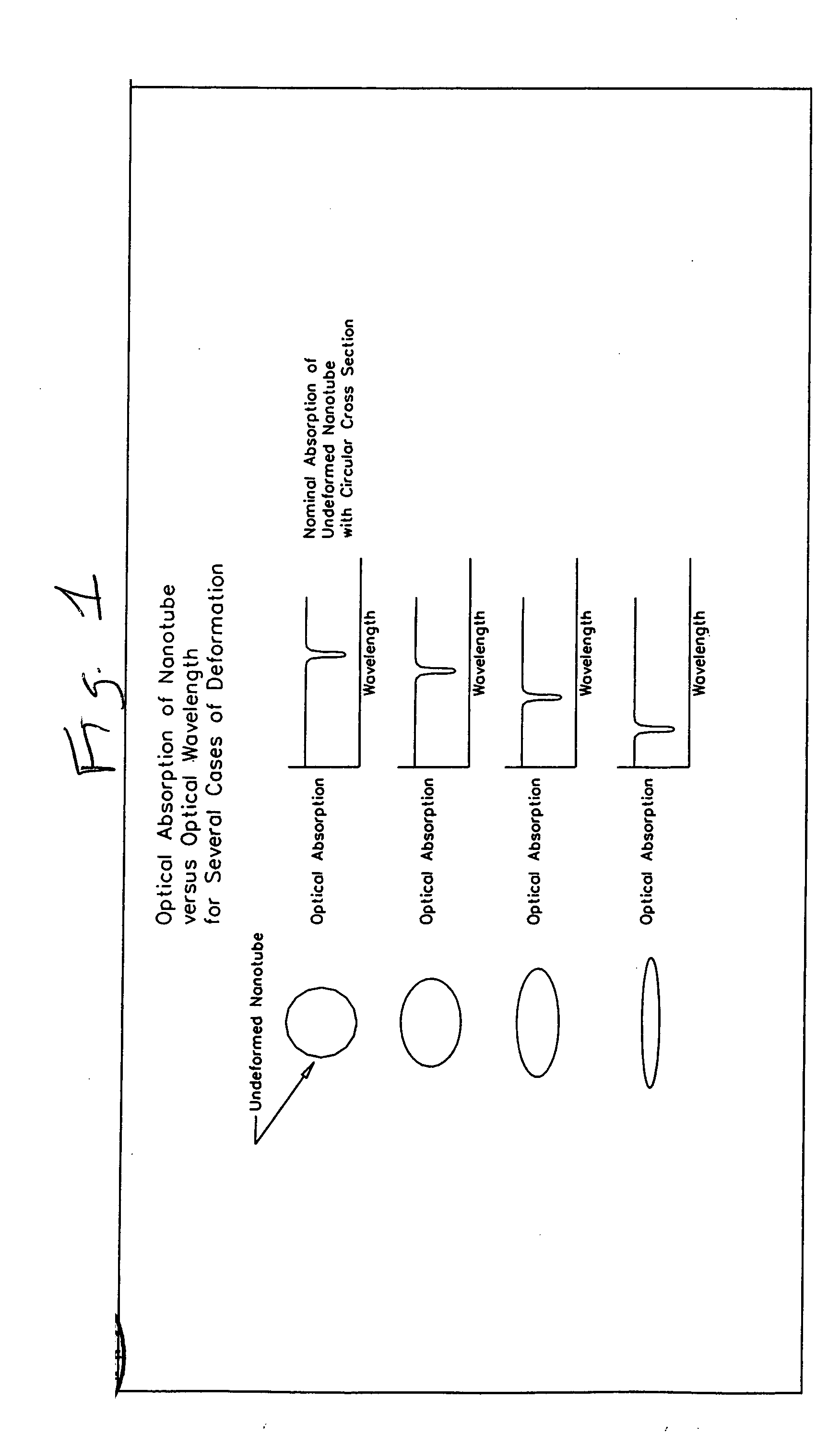
[0044] A first preferred embodiment will now be set forth with reference to FIGS. 1 and 2. FIG. 1 shows the optical absorption spectrum of a carbon nanotube as a function of the degree of deformation. The left column shows various states of deformation, from no deformation at all (top) to extreme deformation (bottom). The right column shows the absorption spectrum for each degree of deformation. The notch, indicating the optical absorption wavelength, moves to the left, indicating absorption at lower wavelengths, as the deformation decreases.

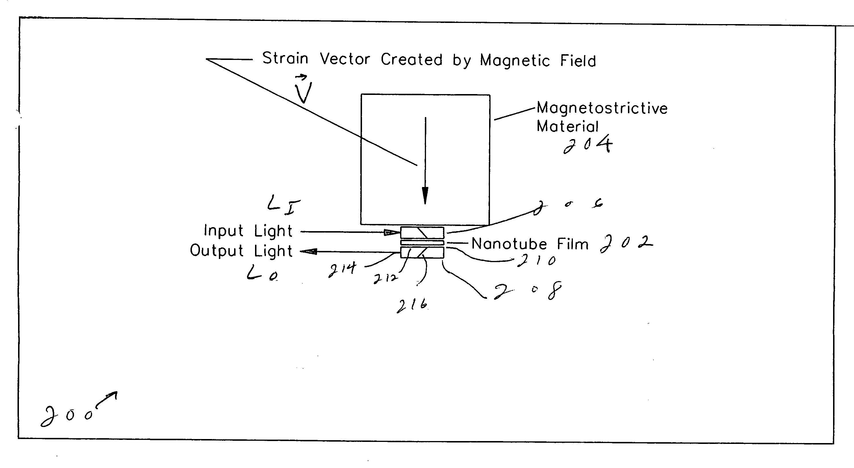
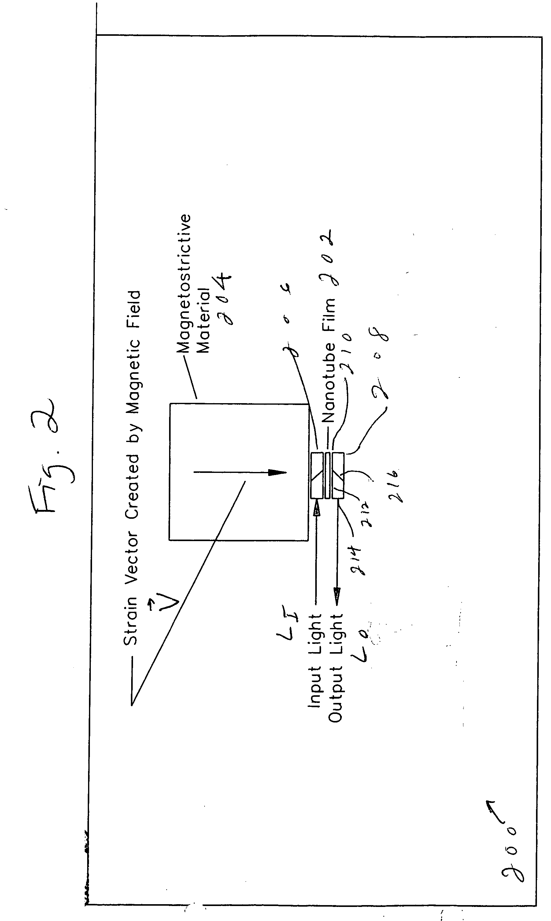
[0045]FIG. 2 shows a magnetic field sensor 200 based on this effect. The parameter to be measured is converted into a physical compression on a nanotube film 202 on an optical surface. In the case of the magnetic field sensor 200, a magnetostrictive material 204...


PUM

PropertyMeasurementUnit
angleaaaaaaaaaa
physical quantityaaaaaaaaaa
semiconductingaaaaaaaaaa

Abstract

A passive optical sensor operates independently of light amplitude by using a semiconducting carbon nanotube material. The material has an optical property dependent on wavelength, e.g., wavelength of absorption, ratio of absorptions at two wavelengths, or fluorescence at one wavelength in response to light at another wavelength. The property is changed by compressing the material or exposing the material to a charge. Light is passed through the material so that the change in the property can be detected.

Description

REFERENCE TO RELATED APPLICATION [0001] The present application claims the benefit of U.S. Provisional Patent Application No. 60 / 533,147, filed Dec. 31, 2003, whose disclosure is hereby incorporated by reference in its entirety into the present disclosure.FIELD OF THE INVENTION [0002] The present invention is directed to a passive optical sensor and more particularly to a passive optical sensor which operates by causing a wavelength-dependent change in the optical characteristics of a carbon nanotube material. DESCRIPTION OF RELATED ART [0003] Fiber optic networks are being developed by the US Air Force and the aerospace industry to control future aircraft in what has been termed the “Fly-by-Fiber” initiative. Essential to the operation of this passive fiber optic network are sensors that measure a variety of parameters required for flight control and other aircraft needs. These sensors must operate in a totally passive mode, where electrical power is not needed to be brought to the...

Claims


Application Information

Patent Timeline
Patent Type & Authority Applications(United States)
IPC IPC(8): G01N21/00G01N21/17G01N21/84
CPCB82Y20/00B82Y30/00G01N21/17G01R33/18G01N21/1717G01N21/64G01N21/84G01N21/1702
Inventor PETTIT, JOHN W.
Owner PETTIT JOHN W
Why Eureka
Try Eureka