Reflective microelectrical mechanical structure (MEMS) optical modulator and optical display system

a micro-electrical mechanical structure and optical modulator technology, applied in the field of optical display systems, can solve the problems of low contrast ratio, reduced brightness of displays, and high cost of optical components, and achieve the effect of reducing the light attenuation or expense of polarizing illumination light and high contrast ratio

Inactive Publication Date: 2005-11-10
MICROSOFT TECH LICENSING LLC
View PDF6 Cites 40 Cited by
  • Summary
  • Abstract
  • Description
  • Claims
  • Application Information

AI Technical Summary

Benefits of technology

[0007] A MEMS optical display system according to the present invention is operable without polarized illumination light, thereby eliminating the light attenuation or expense of the polarizing illumination light. In addition, light can be completely blocked or modulated by cooperation between the MEMS reflectors and the aperture plate, thereby providing display images with very high contrast ratios. Furthermore, such MEMS actuators can be manufactured by conventional CMOS circuit manufacturing processes.
[0079] It will be appreciated that the hysteresis of actuator 170 allows it to be operated and held in its activated downward state without use of storage electrodes 240. Such an operation requires closer tolerances as to the row and column drive voltages and can be more sensitive to process or manufacturing variations that may cause operation failure. Nevertheless, actuator 170 can be operated without storage electrodes 240 to provide a simpler layout and to eliminate the requirement for storage drivers.

Problems solved by technology

Typically, polarization of illumination light greatly attenuates the light, thereby resulting in displays with decreased brightness, or require relatively expensive optical components.
Moreover, such displays commonly have relatively low contrast ratios, which decreases image clarity and overall image quality.
Furthermore, such displays typically require complex or difficult manufacturing processes.

Method used


Image

  • Reflective microelectrical mechanical structure (MEMS) optical modulator and optical display system
  • Reflective microelectrical mechanical structure (MEMS) optical modulator and optical display system
  • Reflective microelectrical mechanical structure (MEMS) optical modulator and optical display system

Examples


Embodiment Construction

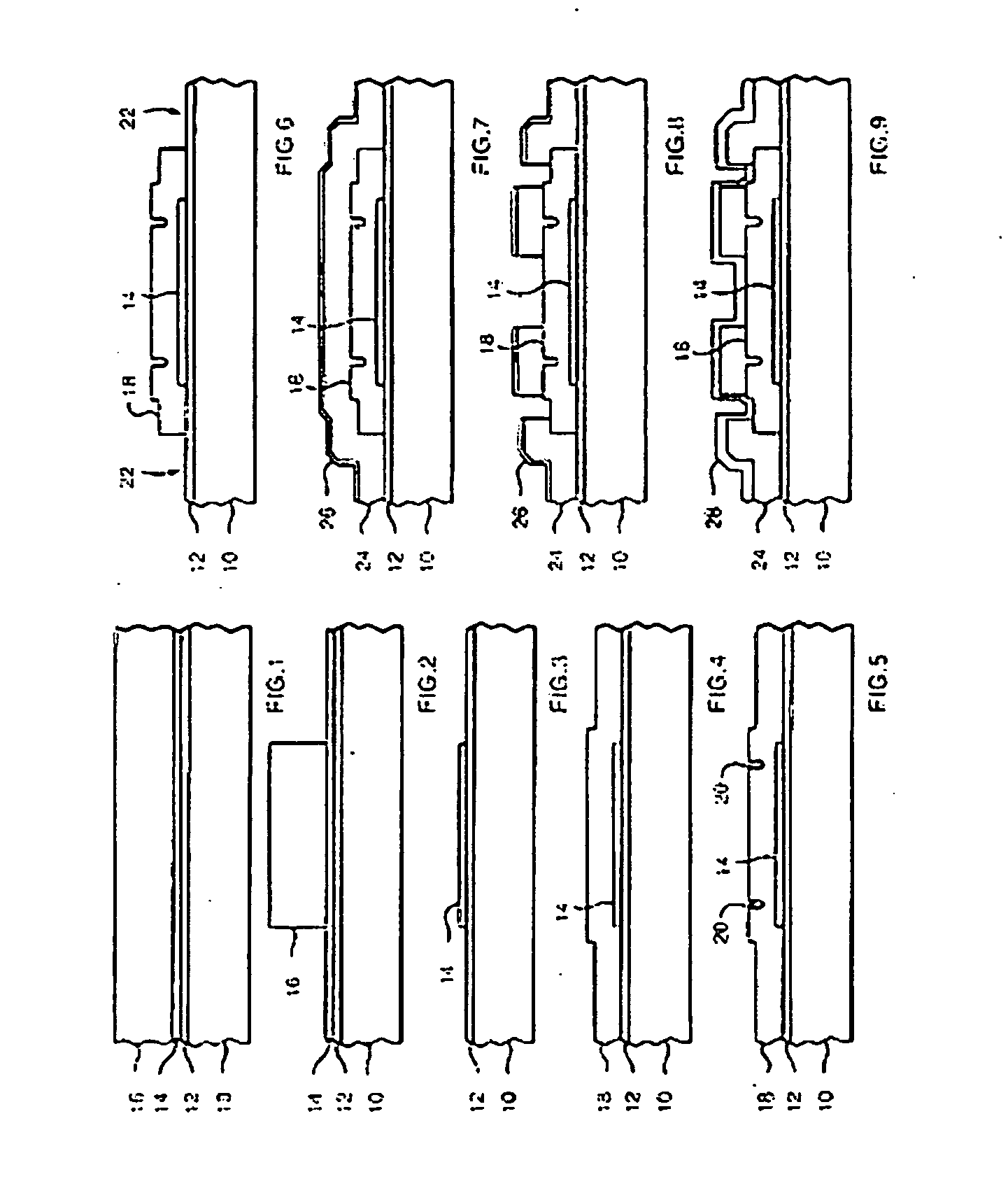
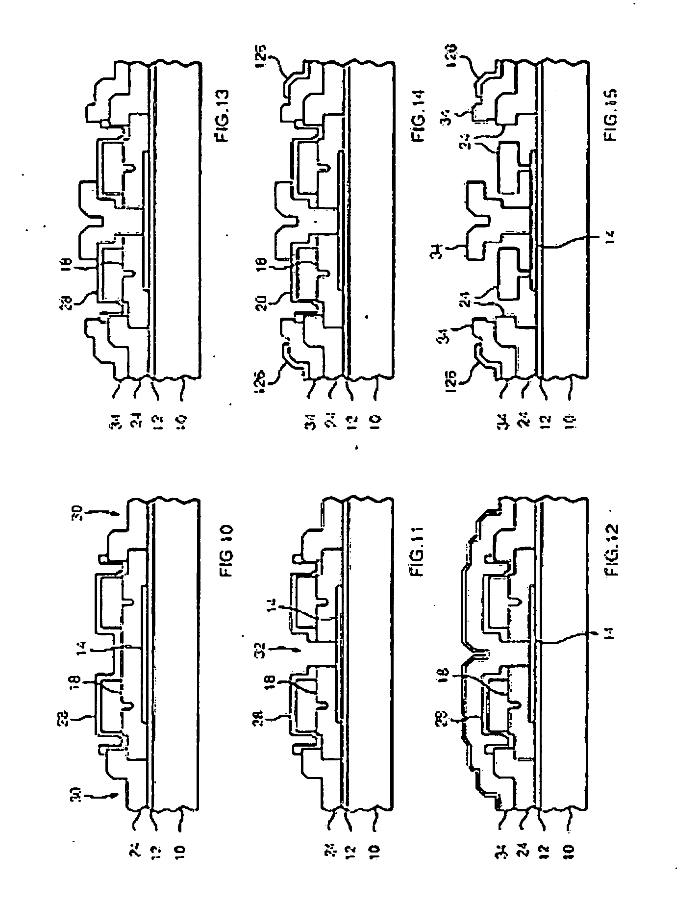
[0020] To assist with understanding the present invention, the general procedure for fabricating micromechanical devices using the MUMPs process is explained with reference to FIGS. 1-15.

[0021] The MUMPs process provides three-layers of conformal polysilicon that are etched to create a desired physical structure. The first layer, designated POLY 0, is coupled to a supporting wafer, and the second and third layers, POLY 1 and POLY 2, respectively, are mechanical layers that can be separated from underlying structure by the use of sacrificial layers that separate layers and are removed during the process.

[0022] The accompanying figures show a general process for building a micro-motor as provided by the MEMS Technology Applications Center, 3021 Cornwallis Road, Research Triangle Park, N.C.

[0023] The MUMPs process begins with a 100 mm n-type silicon wafer 10. The wafer surface is heavily doped with phosphorus in a standard diffusion furnace using POCI 3 as the dopant source. This re...


PUM


Abstract

A MEMS optical display system includes an illumination source for providing illumination light, a collimating lens for receiving the illumination light and forming from it collimated illumination light, and a microlens array having an array of lenslets for receiving the illumination light from the collimating lens. The converging microlens array directs the illumination light through an array of pixel apertures in an aperture plate to a microelectrical mechanical reflector array positioned opposite the aperture plate. The microelectrical mechanical reflector array includes an array of microelectrical mechanical actuators that support reflectors in alignment with the array of pixel apertures and selectively orients the reflectors to direct the illumination light back through the pixel apertures (to form part of a display image) or against the aperture plate (to be blocked). The illumination light passing back through the pixel apertures passes through the microlens array and a beamsplitter to a display screen.

Description

CROSS REFERENCE TO RELATED APPLICATION [0001] This application claims priority to and is a continuation of application Ser. No. 10 / 959,496, filed Oct. 5, 2004, which is a divisional of application Ser. No. 10 / 086,397, filed Mar. 1, 2002, all of which are incorporated herein by reference.FIELD OF THE INVENTION [0002] The present invention relates to optical display systems and, in particular, to a reflective display system that employs a microelectrical mechanical system (MEMS) optical modulator. BACKGROUND AND SUMMARY OF THE INVENTION [0003] Flat panel optical display systems, such as liquid crystal displays, are well known and widely used. Many such displays (e.g., liquid crystal displays) require polarized illumination light. Typically, polarization of illumination light greatly attenuates the light, thereby resulting in displays with decreased brightness, or require relatively expensive optical components. Moreover, such displays commonly have relatively low contrast ratios, whic...

Claims


Application Information

Patent Timeline
Patent Type & Authority Applications(United States)
IPC IPC(8): G02B26/00G02B26/08G02B27/10G02B27/18
CPCY10S359/904G02B26/0841
Inventor STARKWEATHER, GARY K.SINCLAIR, MICHAEL J.
Owner MICROSOFT TECH LICENSING LLC
Why Eureka
Try Eureka