Integrated circuit layout design methodology with process variation bands

a technology of integrated circuit layout and process variation, applied in the field of photolithographic processing, can solve problems such as inability to take into account reliable methods

Active Publication Date: 2005-11-10
SIEMENS PROD LIFECYCLE MANAGEMENT SOFTWARE INC
View PDF99 Cites 481 Cited by
  • Summary
  • Abstract
  • Description
  • Claims
  • Application Information

AI Technical Summary

Benefits of technology

[0008] To address the problems discussed above, the present invention is a method for verifying and/or compensating IC layouts for expected variations that occur in photolithographic processing. In accordance with one embodiment of the present invention, objects to be created on a wafer are modeled to determine ranges in the way the objects would be printed

Problems solved by technology

In the past, there has not been a reliable method of taking into account the process variations that may occur when designing

Method used


Image

  • Integrated circuit layout design methodology with process variation bands
  • Integrated circuit layout design methodology with process variation bands
  • Integrated circuit layout design methodology with process variation bands

Examples


Embodiment Construction

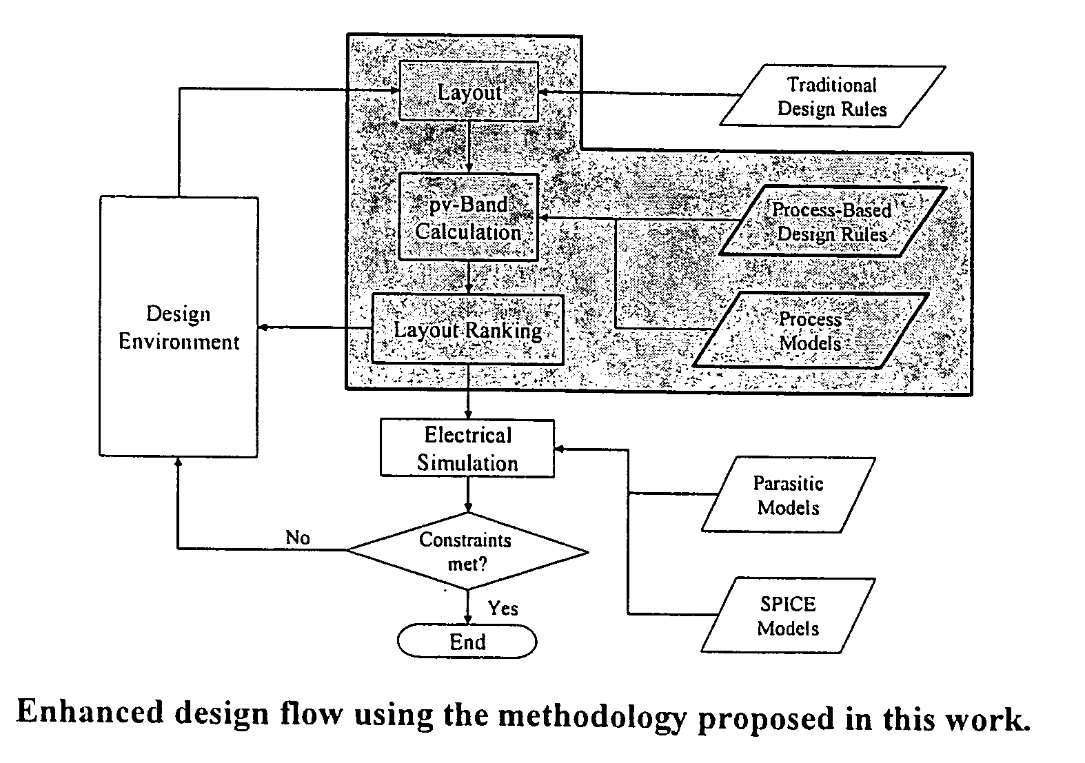
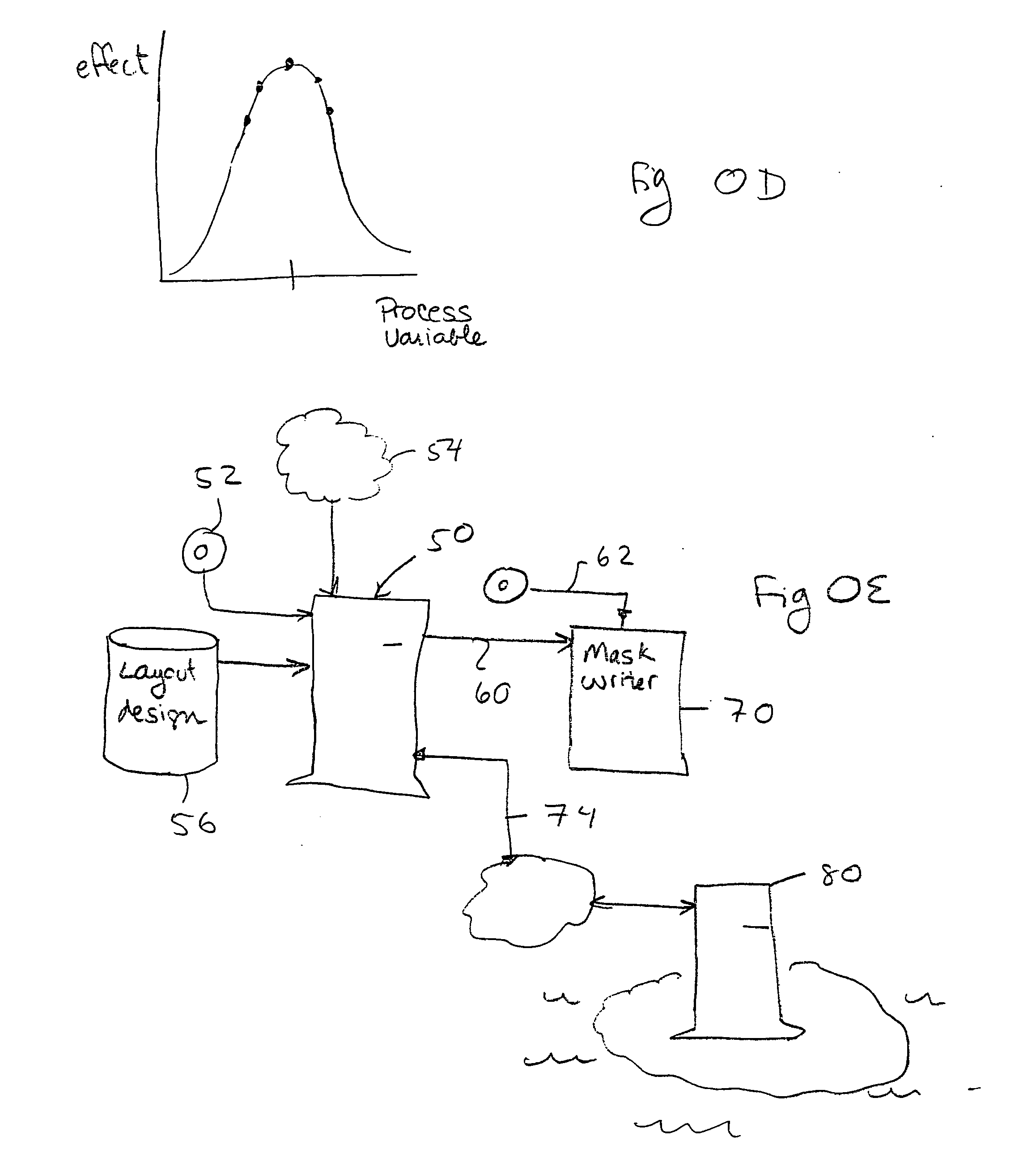
[0056] As indicated above, the present invention is a system for verifying and / or classifying integrated circuit layouts and designs in accordance with anticipated variations in the manufacturing process. Although the present invention is described with respect to the creation of integrated circuits, it will be appreciated that the techniques of the invention can be applied to any manufacturing process that is subject to process variations. Examples of such processes include, but are not limited to mask bias, overlay errors, film stack thickness variations, mask phase errors, post-exposure bake temperatures, resist development times and post exposure bake times. Other devices fabricated lithographically where this invention may be applied may include Micro-electromechanical systems (MEMS), magnetic heads for disk drives, photonic devices, diffractive optical elements, nanochannels for transporting biological molecules, etc.

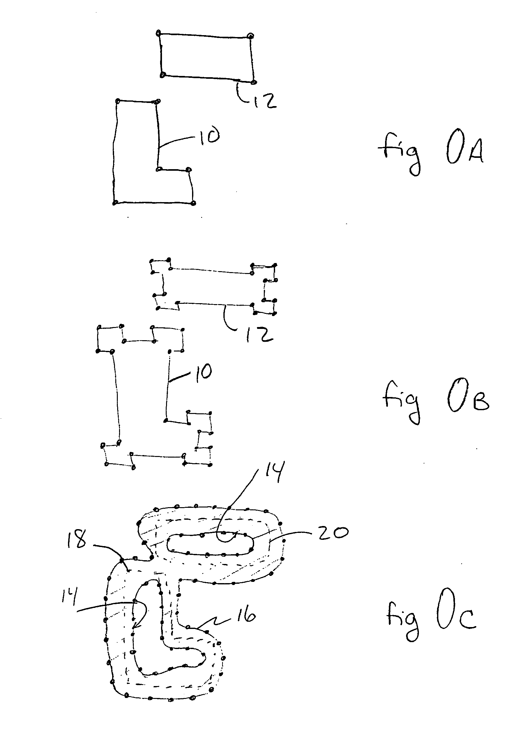
[0057]FIG. 0A illustrates a simplified integrated circuit l...


PUM


Abstract

A system for analyzing IC layouts and designs by calculating variations of a number of objects to be created on a semiconductor wafer as a result of different process conditions. The variations are analyzed to determine individual feature failures or to rank layout designs by their susceptibility to process variations. In one embodiment, the variations are represented by PV-bands having an inner edge that defines the smallest area in which an object will always print and an outer edge that defines the largest area in which an object will print under some process conditions.

Description

CROSS-REFERENCE(S) TO RELATED APPLICATION(S) [0001] The present application claims the benefit of U.S. Provisional Application Nos. 60 / 655,837, filed Feb. 23, 2005, and 60 / 568,849 filed May 7, 2004, which are herein incorporated by reference.FIELD OF THE INVENTION [0002] The present invention relates to photolithographic processing in general, and in particular, to methods of verifying integrated circuit designs for manufacturability due to process variations. BACKGROUND OF THE INVENTION [0003] In a conventional integrated circuit design process, a circuit designer begins with a conceptual idea of what functions an integrated circuit is to perform. The circuit designer then creates a circuit design on a computer and verifies it using one or more simulation tools to ensure that the circuit will operate as desired. The design at this stage may be represented by what is commonly viewed as a circuit schematic, but may also be represented by higher level abstractions within the computer....

Claims


Application Information

Patent Timeline
IPC IPC(8): G03F1/36G06F17/50
CPCG03F1/36G06F17/5022G06F17/5081G06F2217/84G06F2217/06G06F2217/12G06F2217/10G06F30/33G06F30/398G06F2111/08G06F30/367G06F2111/04G06F2119/12G06F2119/18Y02T10/82
Inventor ROBLES, JUAN ANDRES TORRES
Owner SIEMENS PROD LIFECYCLE MANAGEMENT SOFTWARE INC
Why Eureka
Try Eureka