Packaging for optoelectronic devices

a technology of optoelectronic devices and packaging, which is applied in the field of packaging optoelectronic devices, can solve the problems of destroying the device, requiring extra processing steps, and reducing the image capture ability and quality of the device, so as to improve the moisture resistance and reliability, the effect of reducing the cos

Active Publication Date: 2005-11-24
STATS CHIPPAC LTD
View PDF5 Cites 5 Cited by
  • Summary
  • Abstract
  • Description
  • Claims
  • Application Information

AI Technical Summary

Benefits of technology

[0011] The package for optoelectronic devices has a single piece construction with improved moisture resistance, lower cost, and higher reliability.

Problems solved by technology

For example, the glass covers can separate from the plastic or ceramic packaging material resulting in the optoelectronic sensor being exposed to the external environment thereby eventually destroying the device.
Another problem is that moisture can enter the package causing condensation on the inside of the glass cover thus degrading the image capturing ability and quality of the device.
Additionally, the finished package consists of two pieces requiring the device to pass through the normal semiconductor wire bonding process, a cleaning process, and an assembly process to install the glass cover making the production cost of the conventional device high as well as requiring extra processing steps.
Solutions to these problems have been long sought but prior developments have not taught or suggested any solutions and, thus, solutions to these problems have long eluded those skilled in the art.

Method used


Image

  • Packaging for optoelectronic devices
  • Packaging for optoelectronic devices
  • Packaging for optoelectronic devices

Examples


Embodiment Construction

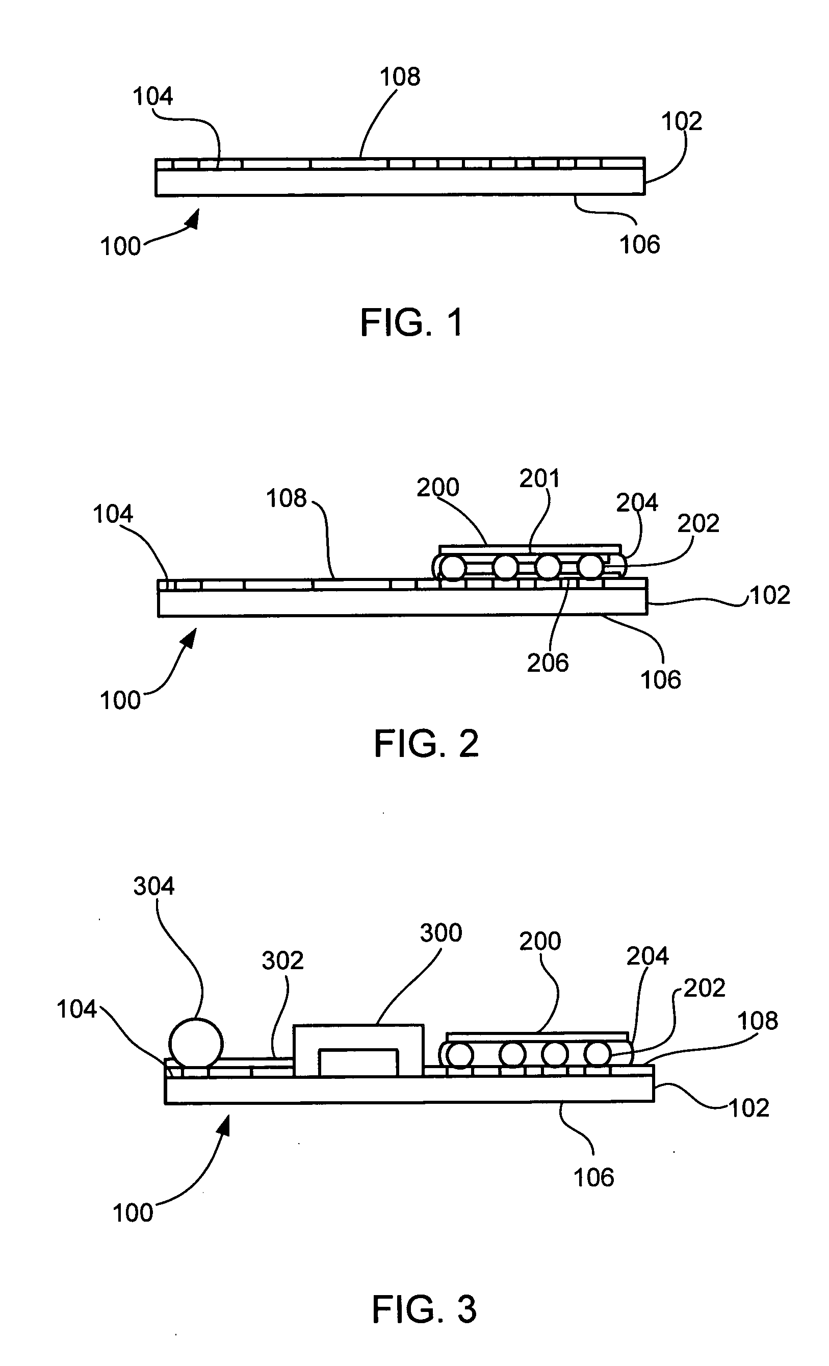
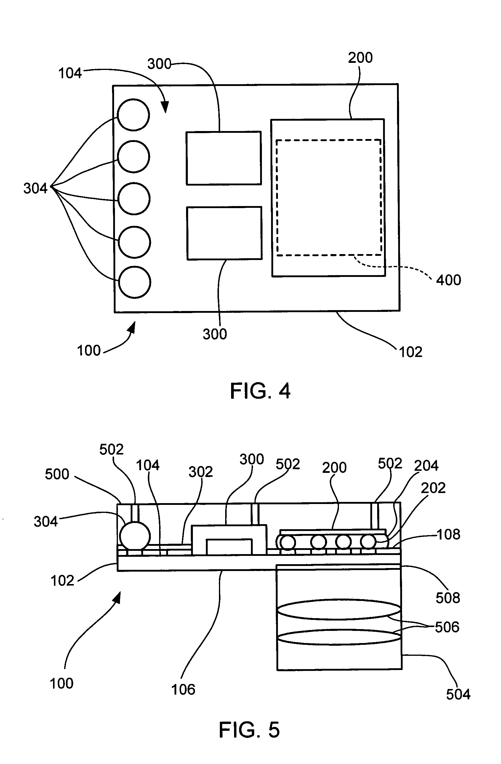
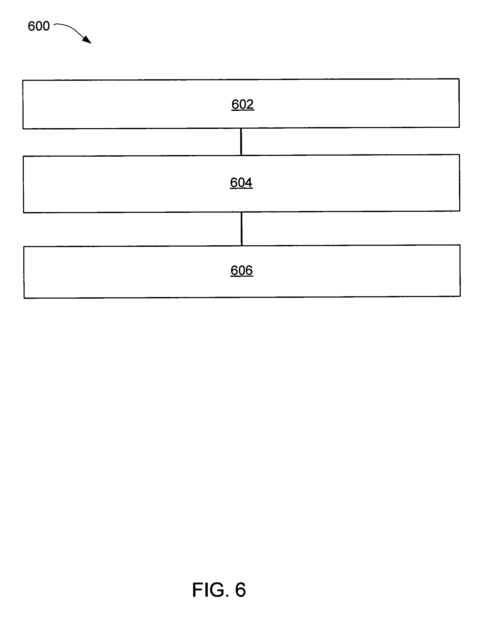
[0019] In the following description, numerous specific details are given to provide a thorough understanding of the invention. However, it will be apparent that the invention may be practiced without these specific details. In order to avoid obscuring the present invention, some well-known system configurations and process steps are not disclosed in detail.

[0020] Likewise, the drawings showing embodiments of the device are semi-diagrammatic and not to scale and, particularly, some of the dimensions are for the clarity of presentation and are shown greatly exaggerated in the FIGs.

[0021] The term “horizontal” as used herein is defined as a plane parallel to the conventional plane or surface of the substrate, regardless of its orientation. The term “vertical” refers to a direction perpendicular to the horizontal as just defined. Terms, such as “on”, “above”, “below”, “bottom”, “top”, “side” (as in “sidewall”), “higher”, “lower”, “over”, and “under”, are defined with respect to the ho...


PUM

PropertyMeasurementUnit
thicknessesaaaaaaaaaa
transparentaaaaaaaaaa
optically transparentaaaaaaaaaa

Abstract

An optoelectronic sensor is attached to an optically transparent substrate, such as glass, and encapsulated to form an optoelectronic device. An optical assembly can be mounted opposite the optoelectronic sensor. Filters and refractive index matching materials may be included between the optoelectronic sensor and the optically transparent substrate.

Description

TECHNICAL FIELD [0001] The present invention relates generally to optoelectronic devices and more particularly to a method and apparatus for packaging optoelectronic devices. BACKGROUND ART [0002] Numerous electronic devices, such as digital cameras, personal digital assistants, and internet appliances, utilize optoelectronic sensors. Optoelectronic sensors are semiconductor chips that are capable of electronically capturing visual information by converting light to electronic signals so that this information can be processed or viewed electronically. Optoelectronic devices, such as image sensors, charge coupled devices (CCDs), or other light sensitive sensors, require the sensors to have a “line of sight” through the package housing the optoelectronic sensors. [0003] A conventional optoelectronic device usually encapsulates a semiconductor chip onto which the sensor is mounted in a package with a non-transparent molded resin or ceramic material, which prevents the encapsulated semi...

Claims


Application Information

Patent Timeline
Patent Type & Authority Applications(United States)
IPC IPC(8): G02B6/30
CPCH01L27/14618H01L27/14625H01L2924/01079H01L2224/16H01L2924/01078H01L27/14683
Inventor KOSSIVES, DEAN PAULRAMAKRISHNA, KAMBHAMPATILAW, EDWARD LAP ZAKSAHAKIAN, DIANETESSIER, THEODORE G.LING, JAMIN
Owner STATS CHIPPAC LTD
Why Eureka
Try Eureka