

Capacitor-built-in-type printed wiring substrate printed wiring substrate, and capacitor
a printed wiring substrate and capacitor technology, applied in the direction of printed circuit non-printed electric components association, printed circuit details, semiconductor/solid-state device details, etc., can solve the problems of extremely low resistance and inductance involved in connection, and achieve the effect of easy connection
- Summary
- Abstract
- Description
- Claims
- Application Information
AI Technical Summary
Benefits of technology
Problems solved by technology
Method used
Image

Examples
embodiment 1
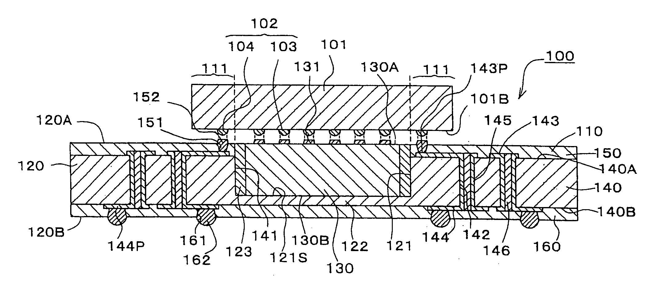
[0108] A first embodiment of the present invention will next be described with reference to the accompanying drawings. Referring to FIG. 1, a capacitor-built-in-type printed wiring substrate 100 of the present invention on which an IC chip is mounted includes an IC chip 101 and a capacitor-built-in-type printed wiring substrate 110 on which the IC chip 101 is mounted.
[0109] The IC chip 101 includes a number of hemispheric connection terminals 102 formed on a lower surface 101B serving as a connection plane. The connection terminals 102 assume the form of a solder bump made of high-melting-point solder. The connection terminals 102 which are located at a substantially central portion in FIG. 1 serve as connection-to-capacitor bumps 103 to be connected to a capacitor 130, which will be described later. The connection terminals 102 which are located around (in FIG. 1, at the right and left sides of) the connection-to-capacitor bumps 103 serve as connection-to-substrate bumps 104 to be...
modified embodiment 1
[0151] In above-described embodiment 1, the insulating resin layer 150 which also serves as a solder resist layer is formed only on the printed wiring substrate 120. However, simultaneously, the insulating resin layer 150 may also be formed on the upper surface 130A of the capacitor 130. Also, according to embodiment 1, after formation of the wiring layers 143 and 144, the through-hole conductors 145, and the insulating resin layers 150 and 160, the capacitor 130 is disposed in the depression 121 (141). However, after the capacitor 130 is disposed in the depression 141, the wiring layers and other components may be formed.
[0152] Specifically, as shown in FIG. 7(a), a capacitor 230 is disposed in the depression 141 of the core substrate 140 shown in FIG. 4(d). Notably, the capacitor 230 is similar to the above-described capacitor 130 except that the thickness (dimension between an upper surface 230A and a lower surface 230B) thereof is slightly less than that of the capacitor 130.
[...
modified embodiment 2
[0162] Embodiment 1 and modified embodiment 1 are described above while mentioning a printed wiring substrate in which a single insulating resin layer 150 (250) is formed on the upper surface of a core substrate, and a single insulating resin layer 160 (260) is formed on the lower surface of the core substrate. However, a plurality of insulating resin layers may be formed on either side of the core substrate. For example, as shown in FIG. 10, three insulating resin layers 351, 352, and 353 (361, 362, and 363) may be formed on the upper (lower) surface of a core substrate 340—which is formed in a manner similar to that in which the core substrate 140 of embodiment 1 is formed-by means of a known buildup process, thereby forming a printed wiring substrate 320 in which a closed-bottomed capacitor accommodation cavity 321 is formed.
[0163] The printed wiring substrate 320 includes connection-to-IC substrate bumps 354 formed on its upper surface (first substrate main-surface) 320A, and c...
PUM
 Abstract
Description
Claims
Application Information