Semiconductor memory device and signal processing system

Inactive Publication Date: 2005-11-24
SONY CORP
View PDF7 Cites 6 Cited by
  • Summary
  • Abstract
  • Description
  • Claims
  • Application Information

AI Technical Summary

Benefits of technology

[0040] According to an embodiment of the present invention, for example, by providing a plurality of address holding portion in a bank, the next address is previously held in the reserved address holding portion. The data is read out from the cell array according to an address held in the current address holding portion and is held in the data holding portion. Then, when it becomes possible to transfer the read out data to the outside at a predetermined timing, the reserved address held in the reserved address holding portion is held in the current address holding portion. This time the data is read out and held

Problems solved by technology

However, general NAND type flash memories have the disadvantage that the read transfer speed is slow due to the following in addition to the long random access time.
When the inside of the page corresponding to a certain address finishes being read, the established data is stored in the data regis

Method used


Image

  • Semiconductor memory device and signal processing system
  • Semiconductor memory device and signal processing system
  • Semiconductor memory device and signal processing system

Examples


Example

[0058] Below, an explanation will be given of preferred embodiments of the present invention with reference to the drawings.

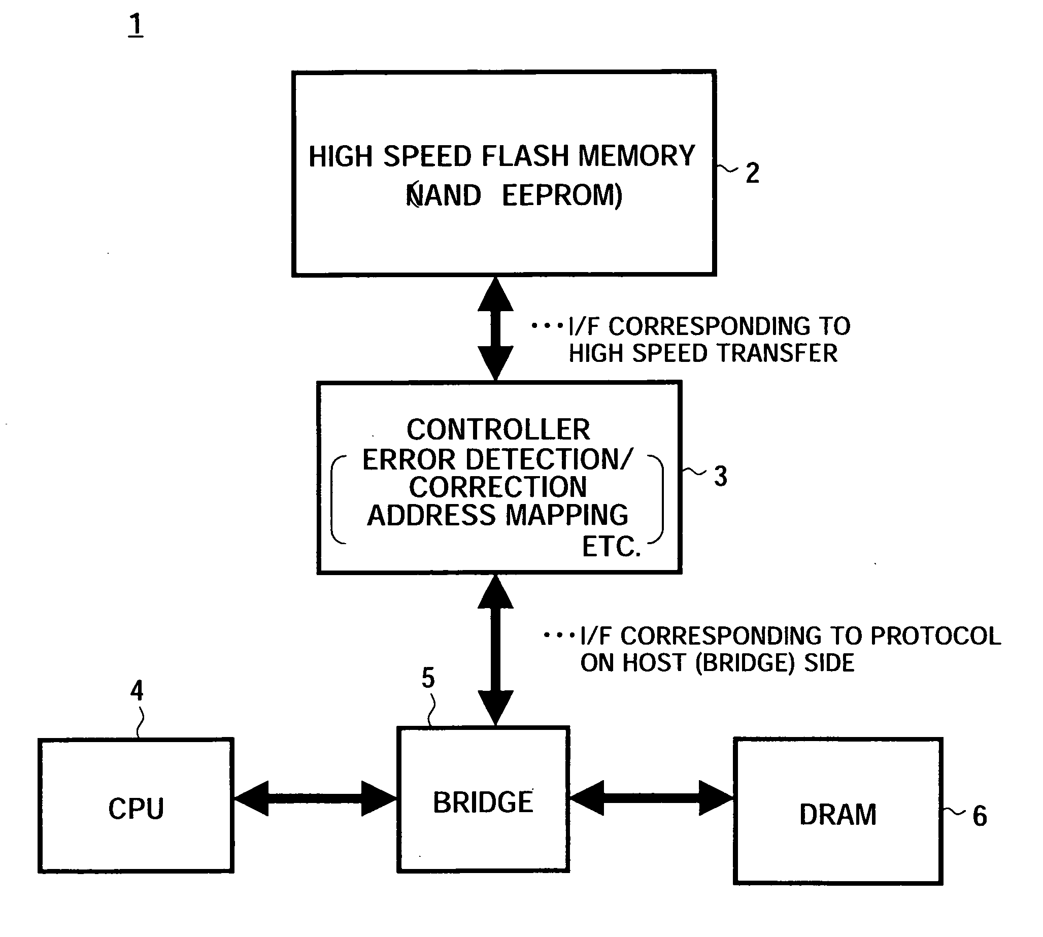
[0059]FIG. 1 is a block diagram of the overall configuration of a signal processing system employing a semiconductor memory device according to an embodiment of the present invention. In the present embodiment, as the semiconductor memory device, a NAND type flash memory in which memory strings formed by connecting pluralities of memory cells in series are connected to bit lines and source lines via selection switches is employed.

[0060] The signal processing system 1 has, as shown in FIG. 1, NAND type flash memory 2 as a first semiconductor memory device, a controller 3, a central processing unit (CPU) 4 as a host device, a bridge circuit 5, and for example a dynamic random access memory as a second semiconductor memory device (DRAM) 6.

[0061] In the signal processing system 1, the host side CPU 4 and the NAND type flash memory 2 are connected via the control...


PUM


Abstract

A semiconductor memory device able to read out data at a high speed continuously, provided with, corresponding to a plurality of banks, current address registers for holding addresses for reading data of cell arrays, reserved address registers able to receive in advance and hold reserved addresses for next read operations from the outside, and bank control circuits for making the current address registers hold reserved addresses held in the reserved address registers, making the data be read out, and making the data latch circuits hold the data when the data read out from the cell arrays of the banks by addresses held in the current address registers and held in the data latch circuits become able to be transferred to the outside, and a signal processing system relating to the same.

Description

CROSS REFERENCES TO RELATED APPLICATIONS [0001] The present invention contains subject matter related to Japanese Patent Application No. 2004-148080 filed in the Japan Patent Office on May 18, 2004 and Japanese Patent Application No. 2004-284036 filed in the Japan Patent Office on Sep. 29, 2004, the entire contents of which being incorporated herein by reference. BACKGROUND OF THE INVENTION [0002] 1. Field of the Invention [0003] The present invention relates to a NAND type flash memory or other semiconductor memory device having memory strings connected to bit lines and source lines via selection switches and to a signal processing system provided with such a semiconductor memory device, more particularly relates to an increase of speed of a read operation of a semiconductor memory device. [0004] 2. Description of the Related Art [0005] In a NAND type flash memory, a plurality of memory transistors are connected in series to form memory strings. Two memory strings share one bit con...

Claims


Application Information

Patent Timeline
IPC IPC(8): G11C7/10G11C8/06G11C11/18G11C16/04G11C16/26
CPCG11C7/1012G11C7/1039G11C7/1051G11C7/106G11C2207/107G11C8/06G11C16/0483G11C16/26G11C7/1063G11C16/06G11C16/08G11C16/12G11C16/32
Inventor YAMANAKA, HIDETOSHINISHIHARA, TOSHIYUKIATSUMI, SHIGERUYOSHIOKA, DAISUKE
Owner SONY CORP
Why Eureka
Try Eureka