Phase-change memory device having a barrier layer and manufacturing method

a technology of phase-change memory and barrier layer, which is applied in the direction of semiconductor devices, electrical appliances, transistors, etc., can solve the problems of affecting the operation of memory programming, and affecting the accuracy of memory programming, so as to achieve stable operation and prolong the operation life

Active Publication Date: 2005-12-01
SAMSUNG ELECTRONICS CO LTD
View PDF23 Cites 33 Cited by
  • Summary
  • Abstract
  • Description
  • Claims
  • Application Information

AI Technical Summary

Benefits of technology

[0007] A phase-change memory device has an oxidation barrier layer to protect against memory cell contamination or oxidation and a method of manufacturing the same. In one embodiment, a semiconductor memory device comprises a molding layer overlying a semiconductor substrate. The molding layer has a protrusion portion vertically extending from a top surface thereof. The device further includes a phase-changeable material pattern adjacent the protrusion portion and a lower electrode electrically connected to the phase-changeable material pattern. According to one aspect of the present invention, an oxidation barrier layer may cover an area where a sidewall of the phase-changeable material pattern and a sidewall of the protrusion portion adjoin. More stable operation and a longer operational lifetime of the phase-change memory device are some of the benefits of the present invention.

Problems solved by technology

During a fabrication of the memory device, and during its operational life in use, these interfaces may become contaminated or oxidized.
Since the operation of phase-changeable memory depends on distinguishing between the memory cell being “on” or “off” based on the cell's resistance to current flow, contamination or oxidation jeopardizes the accuracy of memory programming.

Method used


Image

  • Phase-change memory device having a barrier layer and manufacturing method
  • Phase-change memory device having a barrier layer and manufacturing method
  • Phase-change memory device having a barrier layer and manufacturing method

Examples


Embodiment Construction

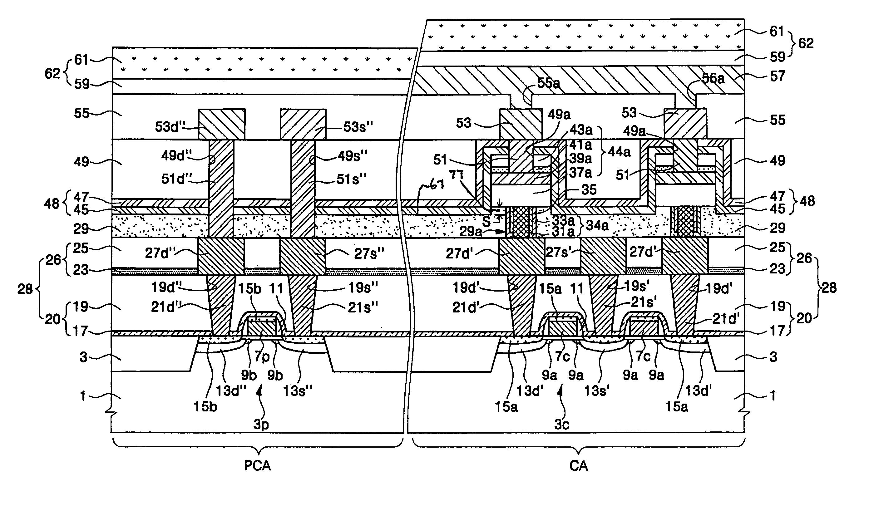
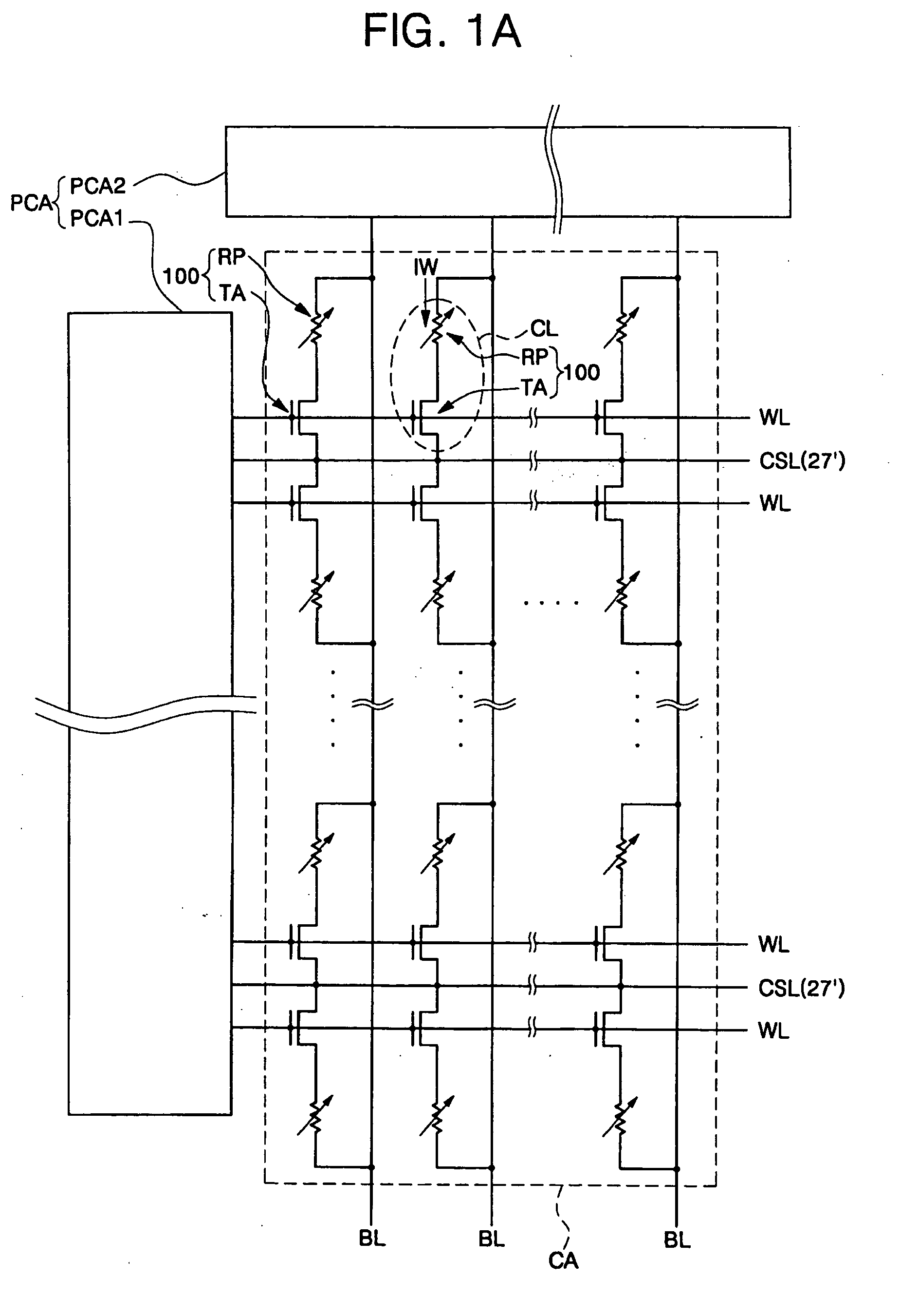
[0015]FIG. 1a is a schematic view of an embodiment that features a phase-change memory cell array CA and a peripheral circuit area PCA of the present invention. The cell array area CA comprises an array of memory cells CL each of which in turn comprises an access transistor TA and a phase-change resistor RP. Each memory cell CL is connected to a bit line BL, a word line WL, and a common source line CSL in a configuration that is known in the art. Other conventional structures will be included in the present invention. For example, the peripheral circuit area PCA includes first and second integrated circuits PCA1, PCA2 to drive the memory cells CL. The state of a memory cell CL is determined by a current sensing of a writing current IW. The current sensing and other functions of memory control are known to one skilled in the art.

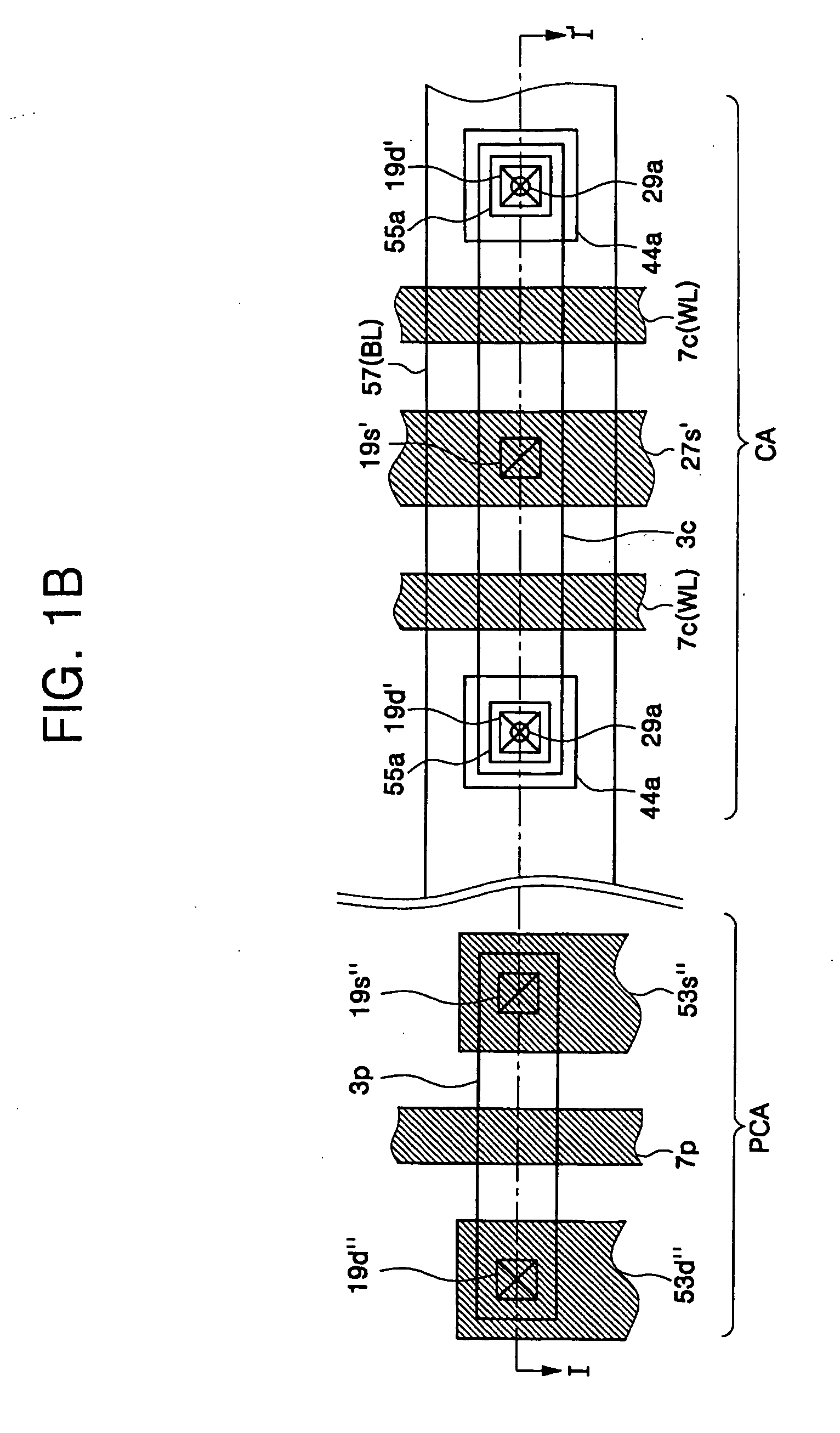
[0016]FIG. 1b is a plan view of a portion of the phase-change memory cell array area CA and a portion of the peripheral circuit area PCA according to an emb...


PUM


Abstract

A phase-change memory device has an oxidation barrier layer to protect against memory cell contamination or oxidation and a method of manufacturing the same. In one embodiment, a semiconductor memory device comprises a molding layer overlying a semiconductor substrate. The molding layer has a protrusion portion vertically extending from a top surface thereof. The device further includes a phase-changeable material pattern adjacent the protrusion portion and a lower electrode electrically connected to the phase-changeable material pattern.

Description

[0001] This application claims priority from Korean Patent Application No. 2004-37965, filed on May 27, 2004, the disclosure of which is incorporated herein in its entirety by reference. BACKGROUND OF THE INVENTION [0002] 1. Field of the Invention [0003] The invention relates to a semiconductor memory device and methods of fabricating the same, and more particularly, to a phase-change memory device and methods of fabricating the same. [0004] 2. Description of Related Art [0005] The use of phase-changeable materials for electronic memory applications is known in the art and is disclosed, for example, in U.S. Pat. No. 6,147,395 and U.S. Pat. No. 6,337,266. The two states of a memory, in the case of phase-changeable memory, depend on the resistance to current flow in a memory cell. The phase-changeable material typically has an amorphous phase and a crystalline phase, with inherent high and low electrical resistance, respectively. The amorphous phase exists at relatively high temperatu...

Claims


Application Information

Patent Timeline
Patent Type & Authority Applications(United States)
IPC IPC(8): H01L27/108H01L27/24H01L45/00
CPCH01L29/7843H01L45/06H01L45/1233H01L27/2436H01L45/144H01L45/1666H01L45/126H10B63/30H10N70/8413H10N70/231H10N70/061H10N70/8828H10N70/826
Inventor HWANG, YOUNG-NAMKOH, GWAN-HYEOBAHN, SU-JINCHO, SUNG-LAELEE, SE-HORYOO, KYUNG-CHANGJEONG, CHANG-WOOKLEE, SU-YOUNKUH, BONG-JIN
Owner SAMSUNG ELECTRONICS CO LTD
Why Eureka
Try Eureka