Thick laser-scribed GaN-on-sapphire optoelectronic devices

a technology of optoelectronic devices and laser scribed gans, which is applied in the direction of semiconductor/solid-state device details, manufacturing tools, welding/soldering/cutting articles, etc., can solve the problems of large kerf width to the wafer, and the fracture of the scribe line on either side of the wafer

Inactive Publication Date: 2005-12-01
GELCORE LLC (US)
View PDF9 Cites 45 Cited by
  • Summary
  • Abstract
  • Description
  • Claims
  • Application Information

AI Technical Summary

Problems solved by technology

After the scribe lines are created, applying a force on either side of the scribe line fractures the wafer.
However, dicing saws introduce a large kerf width to the wafer, corresponding to wide streets and fewer device die yielded per wafer.

Method used


Image

  • Thick laser-scribed GaN-on-sapphire optoelectronic devices
  • Thick laser-scribed GaN-on-sapphire optoelectronic devices

Examples


Embodiment Construction

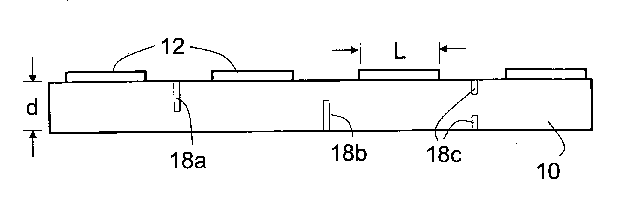
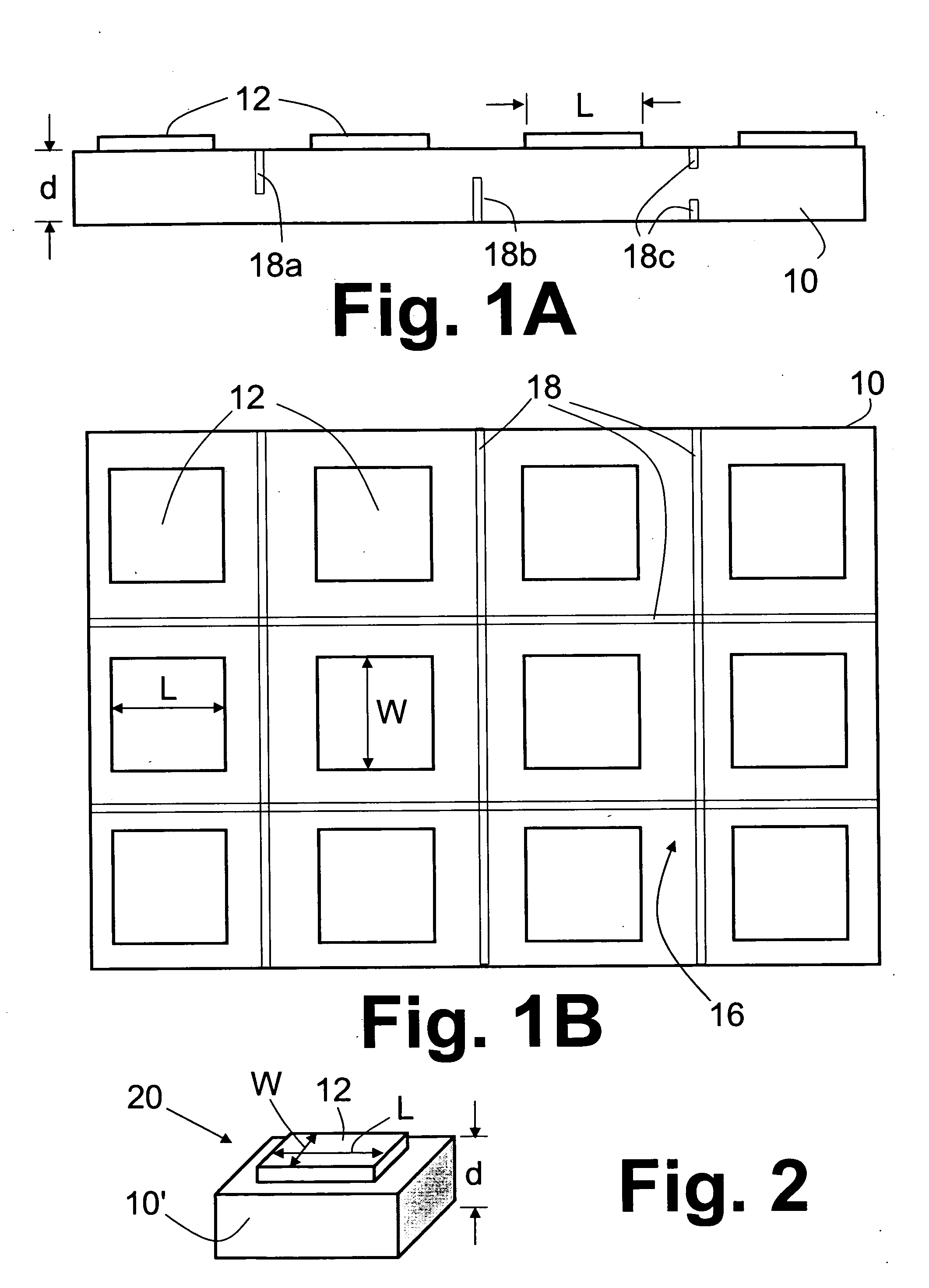
[0011] The following relates to optoelectronic devices, such as devices made from GaN-based semiconductor material, disposed on a thick sapphire substrate, formed via laser scribes on one or both sides of the chip. The typical device thickness is between 125 to 600 micron.

[0012] With reference to FIGS. 1A and 1B, a sapphire substrate 10 has a plurality of electronic or optoelectronic devices 12 disposed thereon. The sapphire substrate has a thickness d of greater than 125 microns. In some embodiments the substrate thickness d is less than 600 microns. Lateral dimensions L, W of each device 12 are in some embodiments 350 micron per side or greater. The dimensions L and W need not be the same, and moreover each device 12 can have a lateral shape other than the illustrated rectangular shape; for example, the devices can have a circular, elliptical, triangular, or otherwise-shaped area.

[0013] In some embodiments, the devices 12 are GaN-based light emitting diode (LED) devices formed b...


PUM

PropertyMeasurementUnit
thicknessaaaaaaaaaa
thicknessaaaaaaaaaa
thicknessaaaaaaaaaa

Abstract

A sapphire wafer having a thickness greater than 125 microns and having devices disposed thereon is laser scribed to form a grid array pattern of laser scribe lines laser scribed into the sapphire wafer. The sapphire wafer is separated along the laser scribe lines to separate a plurality of device dice defined by the grid array pattern of laser scribe lines. Each device die includes (i) a device and (ii) a portion of the sapphire wafer having the thickness greater than 125 microns. In some embodiments, a GaN LED device die includes a GaN based LED device, and a sapphire substrate supporting the GaN based LED device. The sapphire substrate has: (i) a thickness greater than 125 microns effective for increased light extraction due to a lower critical angle for total internal reflection; and (ii) sides generated by laser scribing.

Description

[0001] This application claims the benefit of U.S. Provisional Application No. 60 / 568,725 filed May 6, 2004, entitled “Thick Laser-Scribed GaN-on-sapphire Optoelectronic Devices” which is incorporated herein by reference in its entirety.[0002] The following U.S. patents and U.S. published applications: U.S. Patent Appl. Publ. No. 2002 / 0127824 A1, publication date Sep. 12, 2002; U.S. Patent Appl. Publ. No. 2002 / 0177288 A1, publication date Nov. 28, 2002; U.S. Patent Appl. Publ. No. 2003 / 0003690 A1, publication date Jan. 2, 2003; and U.S. Pat. No. 6,413,839 issued Jul. 2, 2002; are each incorporated by reference herein in its entirety. BACKGROUND [0003] The following relates to the light emitting diode (LED) arts. It finds particular application in conjunction with the separation of a plurality of GaN-based light emitting diode (LED) devices formed on or disposed on a sapphire wafer, and with LED device die formed by same, and will be described with particular reference thereto. Howev...

Claims


Application Information

Patent Timeline
Patent Type & Authority Applications(United States)
IPC IPC(8): B23K26/40H01L21/461H01L21/78H01L29/20H01L33/00
CPCB23K26/4075H01L33/0095H01L21/78B23K26/40B23K2103/50
Inventor SHELTON, BRYAN S.VENUGOPALAN, HARI S.LIBON, SEBASTIENELIASHEVICH, IVAN
Owner GELCORE LLC (US)
Why Eureka
Try Eureka