Substrate for organic EL display devices and organic EL display devices

a technology of organic el and display devices, applied in the direction of identification means, instruments, discharge tubes luminescnet screens, etc., can solve the problems of difficult application of aging treatments

Inactive Publication Date: 2005-12-01
KYOCERA CORP
View PDF0 Cites 10 Cited by
  • Summary
  • Abstract
  • Description
  • Claims
  • Application Information

AI Technical Summary

Benefits of technology

[0013] In order to effectively perform the short-circuit aging treatment or the lifetime aging treatment, it is preferred to perform these aging treatments before the cutting step. In order to perform these aging treatments before the cutting step, there has been a proposal wherein wires, which are used for application of a voltage for the aging treatments, and which are connectable to a voltage applying device provided outside organic EL display devices, are disposed on a glass substrate with a large number of organic EL devices formed thereon, and wherein the voltage is collectively applied between the anode strips and between the cathode strips of the organic EL devices (JP-A-2004-146212). The connected state of the anode strips and the connected state of the cathode strips by such wires are eliminated by cutting the wires in the cutting step. By this proposal, it is possible to effectively subject such a large number of organic EL devices to the aging treatments for a short period of time.
[0017] As indicated by dotted lines under the organic EL display device 200 in FIG. 8, it is proposed that a special area 201 is formed on the glass sheet in order to secure the route for electrical connection of the anodes outside the organic EL display device and the route for electrical connection of all cathode circuitous wiring 11 outside the organic EL display device 200, the cathode circuitous wiring existing in the left and right areas. For, e.g., the purpose of avoiding the problem that when an anode and a cathode of an organic EL device is short-circuited during an aging treatment, the voltage applied to the other organic EL devices is lowered, it is preferred to provide a resistive area having a relatively high resistance.
[0020] By fabricating each of organic EL display devices as shown in FIG. 8, it is possible to collectively subject a large number of organic EL display devices to the aging treatment even when each of the organic EL display devices is configured to have wires drawn out of three sides of the organic EL device having a rectangular shape. However, the number of the organic EL display devices cut out of a single glass substrate is decreased since it is necessary to provide the areas 201 that are not utilized as the organic EL display devices. As a result, the production cost of the organic EL display devices is increased.
[0021] It is an object of the present invention to provide a substrate for organic EL display devices and organic EL display devices, which are capable of being collectively subjected to an aging treatment without decreasing the number of the organic EL display devices cut out of a single glass substrate, each of the organic EL display devices being configured to have wires drawn out of three sides of the organic EL device having a rectangular shape.
[0031] In accordance with the present invention, it is possible to collectively subject organic EL display devices to an aging treatment without decreasing the number of the organic EL display devices cut out of a single glass substrate even when each of the organic EL display devices is configured to have wires drawn out of three sides of the organic EL device having a rectangular shape.

Problems solved by technology

However, the proposal stated earlier is difficult to be applied to the aging treatments in some cases.

Method used


Image

  • Substrate for organic EL display devices and organic EL display devices
  • Substrate for organic EL display devices and organic EL display devices
  • Substrate for organic EL display devices and organic EL display devices

Examples


first embodiment

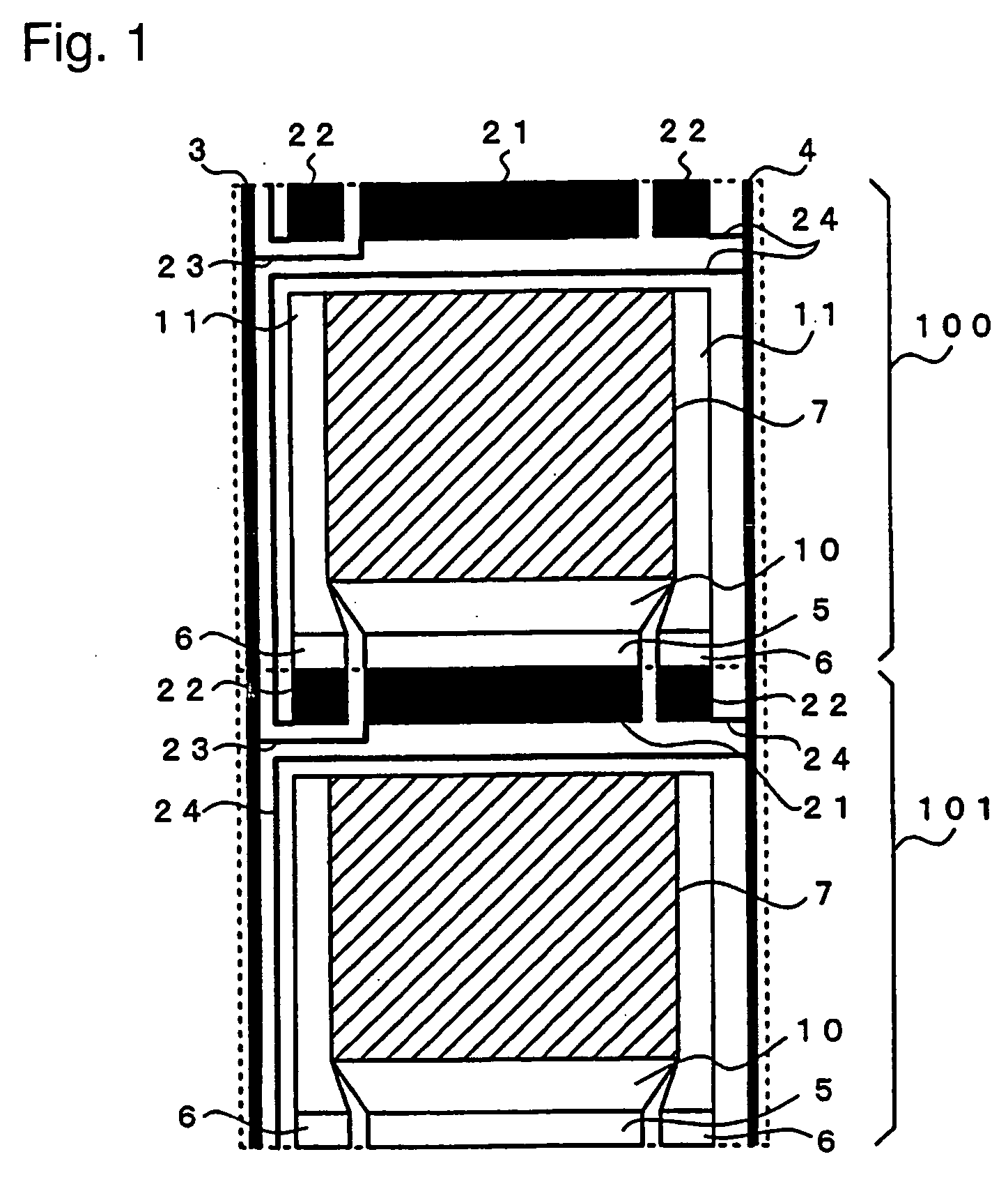
[0041]FIG. 1 is a plan view showing organic EL display devices 100 and 101 according to a first embodiment of the present invention. In FIG. 1, an area surrounded by dotted line indicates the organic EL display device 100 or organic EL display device 101 having a rectangular shape. The rectangular shape means that the largest surface of an organic EL display device is rectangular or substantially rectangular, and that the largest surface may be imperfectly rectangular as long as a first side to a fourth side can be specified.

[0042] Although the only two organic EL display devices 100 and 101 are shown to be fabricated on a glass substrate (not shown) in FIG. 1, a large number of organic EL display devices are fabricated so as to be close to adjacent organic EL display devices in a matrix pattern on the glass substrate as a matter of fact. The structure of all organic EL display devices is the same as the structure of the organic EL display devices 100 and 101 shown in FIG. 1. Each ...

second embodiment

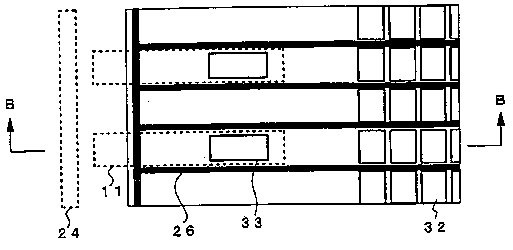
[0067]FIG. 5 is a plan view showing the organic EL display devices 100 and 101 according to a second embodiment of the present invention. In the first embodiment, the cathode-lead wire for aging 24, which connects between the connection resistance at cathode side for aging 22 of the organic EL display device 101 on a side remote from the cathode-common wires for aging 4 and the cathode-common wires for aging 4, is formed outside the cathode circuitous wiring 11 (on a side of the organic EL device 7 remote from the cathode-common wires for aging) in the organic EL display device 100. However, the cathode-lead wire for aging may be formed on an inner side of the cathode circuitous wiring 11 (on a side closer to the organic EL device 7) in the organic EL display 100 as shown in FIG. 5.

[0068]FIG. 6(A) is a plan view showing cathode circuitous wiring 11, the cathode-lead wire for aging 24 and their peripheral areas, and FIG. 6(B) is a cross-sectional view taken along line B-B of FIG. 6(...


PUM


Abstract

A first organic EL display device has cathode-common wires for aging, first and second connection resistances at cathode side for aging, and a cathode-lead wire for aging formed thereon, the cathode-lead wire for aging connecting between a first connection resistance at cathode side for aging on a side remote from the cathode-common wires for aging and the cathode-common wires for aging. The cathode-lead wire for aging is drawn out of the first connection resistance at cathode side for aging, passes outside cathode circuitous wiring in a second organic EL display device adjacent the first organic EL display device, passes through a space defined by the second organic EL display device, first and second connection resistances at cathode side for aging of the second organic EL display device, and a connection resistance at anode side for aging of the second organic EL display device, and is connected to the cathode-common wires for aging.

Description

BACKGROUND OF THE INVENTION [0001] 1. Field of the Invention [0002] The present invention relates to a substrate for organic EL display devices and organic EL display devices, which are capable of being effectively subjected to an aging treatment. [0003] 2. Description of the Related Art [0004] Organic EL (electroluminescence) display devices are current-drive display devices, which emit light by themselves when a current is supplied to the organic EL layers interposed between an anode and a cathode provided so as to be opposite each other. The organic EL display devices are also called organic LEDs because of having characteristics similar to semiconductor light emitting diodes. [0005] Organic EL devices have such a structure that a plurality of anode strips, which is connected to an anode or forms an anode per se, is provided on a glass substrate in parallel with one another, that a plurality of cathode strips, which is connected to a cathode or forms a cathode per se, is provided...

Claims


Application Information

Patent Timeline
Patent Type & Authority Applications(United States)
IPC IPC(8): G09F9/30H01L25/04H05B33/06H01L27/32H01L51/50H05B33/02H05B33/10H05B33/14H05B44/00
CPCG09G3/3216G09G2320/043G09G2330/08H01L25/046H01L27/3281H01L2924/0002H01L2251/562H01L2924/00H10K19/901H10K59/17H10K71/831
Inventor KATO, NAOKI
Owner KYOCERA CORP
Why Eureka
Try Eureka