Structure and method of forming metal buffering layer

a buffer layer and metal technology, applied in the direction of semiconductor devices, electrical equipment, semiconductor/solid-state device details, etc., can solve the problem of reducing and achieve the effect of reducing the probability of circuit trace collapsing and increasing the reliability of packaged wafers

Active Publication Date: 2005-12-01
ADVANCED SEMICON ENG INC
View PDF6 Cites 13 Cited by
  • Summary
  • Abstract
  • Description
  • Claims
  • Application Information

AI Technical Summary

Benefits of technology

[0006] In order to solve the above-mentioned problems, a structure and method of forming a metal buffering layer is provided to reduce the collapsing probability of the circuit trace, and then increase the reliability of the packaged wafer.

Problems solved by technology

The above-mentioned packaging structure often incurs a collapsing problem of the circuit trace 150, and that reduces the reliability of the packaged wafer.

Method used


Image

  • Structure and method of forming metal buffering layer
  • Structure and method of forming metal buffering layer
  • Structure and method of forming metal buffering layer

Examples


Embodiment Construction

[0015] It is necessary to notice that the manufacture processes and the structures described below do not include the complete ones. The present invention can be implemented with any kinds of manufacturing technologies, and only the necessary ones promoting to understand are described in the following.

[0016] The invention will be explained in detail in accordance with the accompanying drawings, it would be known that all drawings below are only in simplified forms and not drawn in proportion to the real cases, further, the dimensions of the drawings are enlarged for explaining and understanding more clearly.

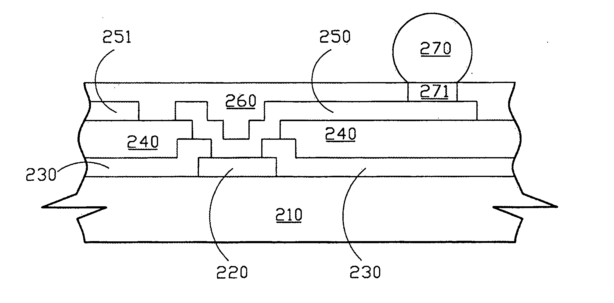
[0017] Referring to FIG. 2, it shows a schematic cross-sectional view of one preferred embodiment of the present invention. A wafer 210 having at least a bonding pad 220 and a passivation layer 230 exposing a portion surface of a bonding pad 220 thereon is provided. In the embodiment, the bonding pad 220, for example, can be an aluminum or copper pad, and the passivation layer ...


PUM

PropertyMeasurementUnit
conductiveaaaaaaaaaa
structureaaaaaaaaaa
dielectricaaaaaaaaaa

Abstract

A structure and method of forming a metal buffering layer during the formation of a redistribution layer is provided. It only changes a mask to form the metal buffering layer and circuit traces simultaneously. The metal buffering layer can increase the flatness of the dielectric layer covering on the metal buffering layer. It can also make the structure under the metal buffering layers suffer uniform pressure to prevent the passivation layer from cracking and the circuit traces from collapsing in order to increase the yield of the packaged chips.

Description

BACKGROUND OF THE INVENTION [0001] 1. Field of the Invention [0002] The present invention relates to a structure and method of forming a buffering layer, and more particularly to a structure and method of forming a metal buffering layer in a manufacture process of a conductive bump. [0003] 2. Description of the Prior Art [0004] Conventionally, the I / O bonding pads are distributed on the surroundings of chips of a wafer, as the original design concerned or for easily printing wires. In order to redistribute the distribution of the I / O bonding pads, a rerouting (or redistribution) technology of the manufacture process of a conductive bump is used for changing the surrounding arrangement into the dispersing arrangement of the bonding pads to achieve the demand of miniaturizing a package size. Referring to FIG. 1, a wafer 110, thereon, has at least a bonding pad 120 and a passivation layer 130 exposing a portion of the bonding pad 120. A dielectric layer 140 covers the passivation layer...

Claims


Application Information

Patent Timeline
Patent Type & Authority Applications(United States)
IPC IPC(8): H01L21/44H01L21/48H01L21/50H01L21/768H01L23/31H01L23/525
CPCH01L23/3114H01L23/525H01L2224/05569H01L2224/0401H01L2924/0002H01L2224/13023H01L2224/05552H01L2224/023H01L2924/0001
Inventor HUANG, TAI-YUAN
Owner ADVANCED SEMICON ENG INC
Why Eureka
Try Eureka