Wired circuit board and connection structure of wired circuit board
a technology of wired circuit board and connection structure, which is applied in the direction of fixed connections, laminating printed circuit boards, coupling device connections, etc., can solve the problems of inability to confirm the connection from the appearance, and inevitable cost of continuity inspection, so as to reduce the burden on the number of processes and reduce the cost caused by the inspection.
- Summary
- Abstract
- Description
- Claims
- Application Information
AI Technical Summary
Benefits of technology
Problems solved by technology
Method used
Image

Examples
example 1
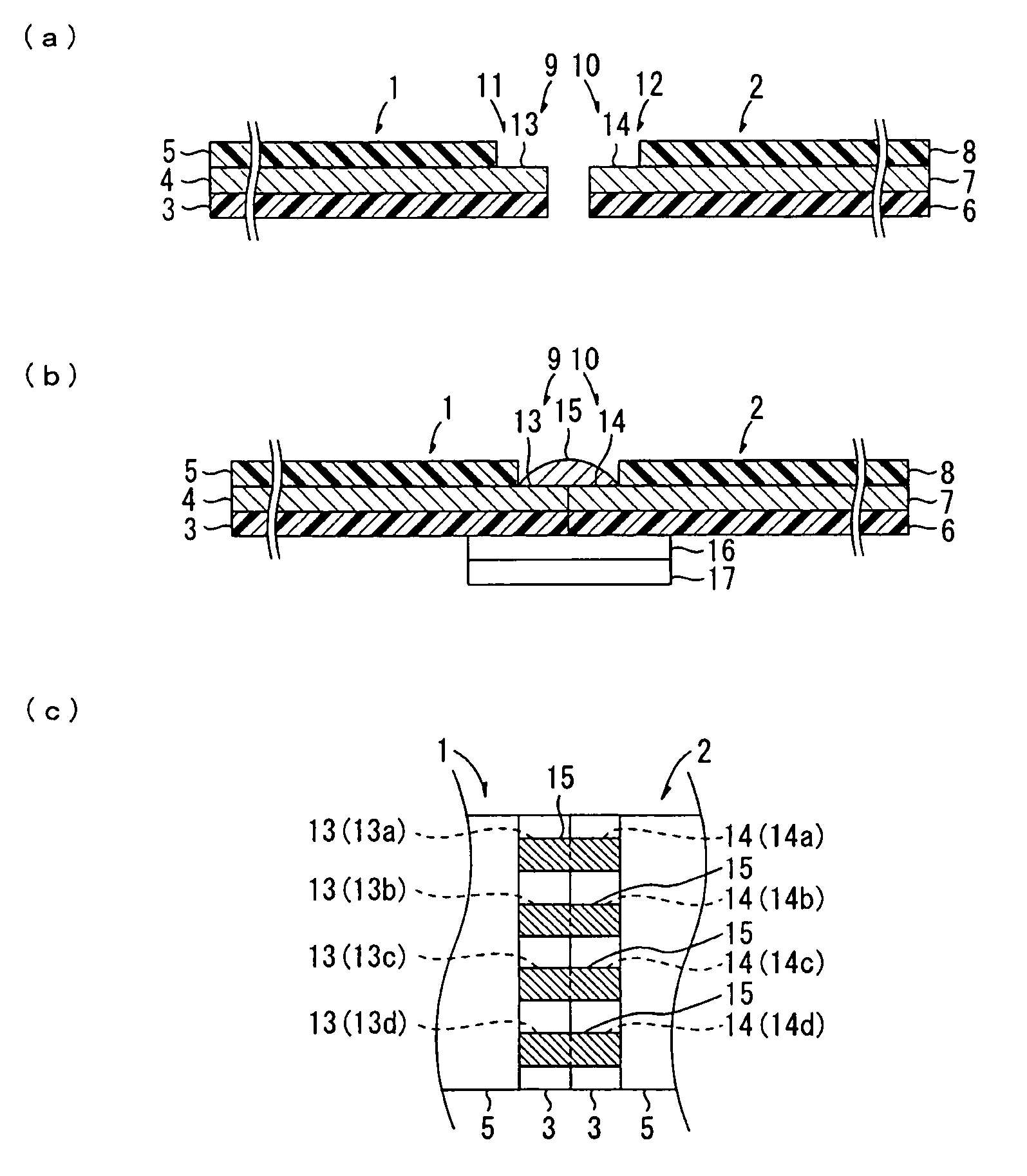
[0083] After a copper foil was affixed to a first base insulating layer composed of a polyimide film having a thickness of 12.5 μm through an epoxy adhesive layer having a thickness of 10 μm, a first conductor pattern composed of a copper wiring having a thickness of 18 μm was formed by a subtractive method. Further, a first cover insulating layer composed of a polyimide film having a thickness of 12.5 μm was laminated on the first conductor pattern through an epoxy adhesive layer having a thickness of 15 μm. A first opening serving as a first connection terminal portion was formed in one end in the longitudinal direction, thereby obtaining a first wired circuit board (see FIG. 1 (a)).
[0084] After a copper foil was affixed to a second base insulating layer composed of a polyimide film having a thickness of 12.5 μm through an epoxy adhesive layer having a thickness of 10 μm, a second conductor pattern composed of a copper wiring having a thickness of 18 μm was formed by a subtractiv...
example 2
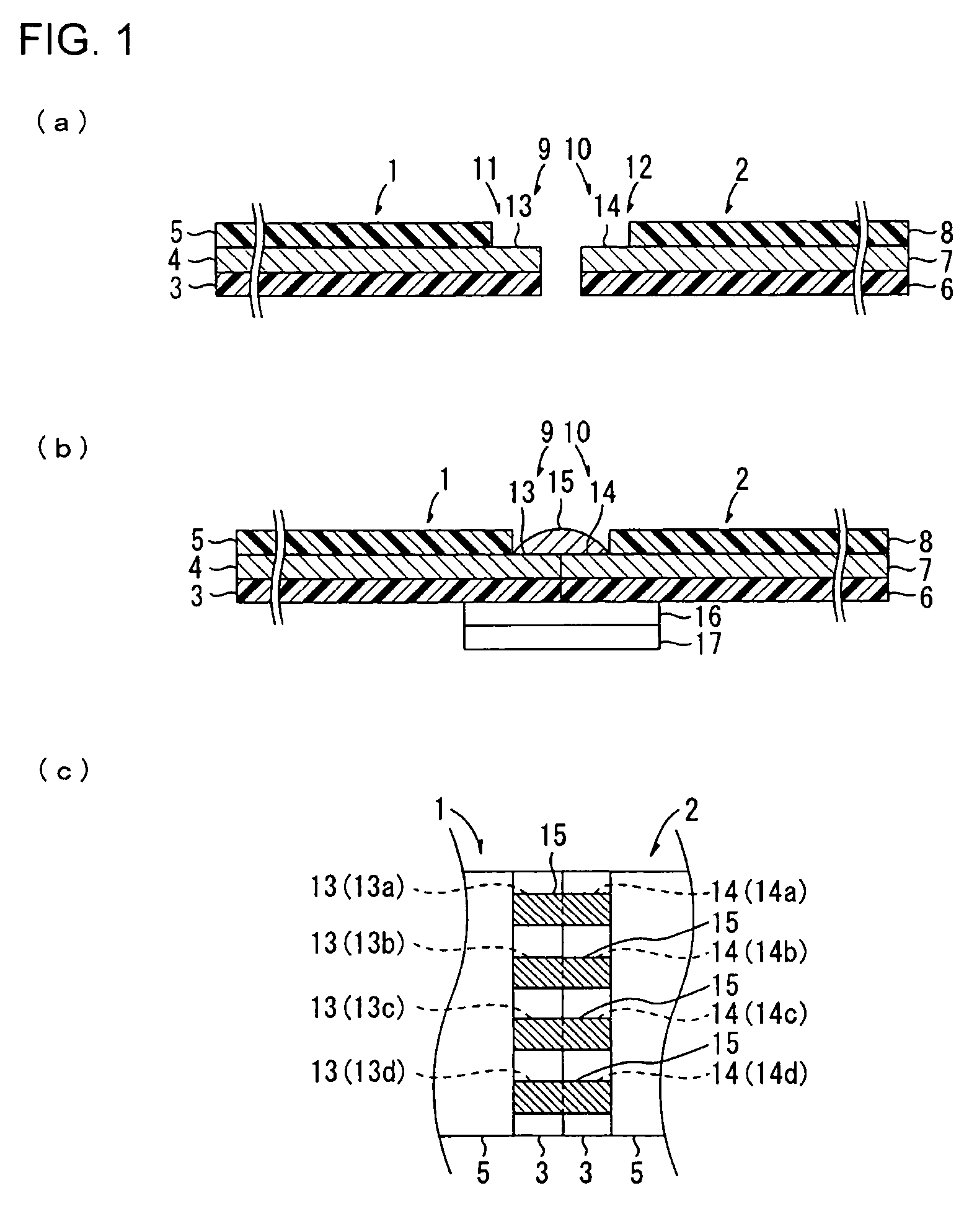
[0087] A first base insulating layer composed of a polyimide film having a thickness of 10 μm, a first conductor pattern composed of a copper wiring having a thickness of 10 μm formed by an additive method, and a first cover insulating layer composed of a polyimide film having a thickness of 5 μm were successively laminated on a supporting substrate composed of a stainless foil having a thickness of 20 μm. A first opening serving as a first connection terminal portion was formed in one end in the longitudinal direction, thereby obtaining a first wired circuit board (see FIG. 2 (a)
[0088] After a copper foil was affixed to a second base insulating layer composed of a polyimide film having a thickness of 12.5 μm through an epoxy adhesive layer having a thickness of 10 μm, a second conductor pattern composed of a copper wiring having a thickness of 18 μm was formed by a subtractive method. Further, a second cover insulating layer composed of a polyimide film having a thickness of 12.5 ...
example 3
[0091] A first base insulating layer composed of a polyimide film having a thickness of 10 μm, a first conductor pattern composed of a copper wiring having a thickness of 10 μm formed by an additive method, and a first cover insulating layer composed of a polyimide film having a thickness of 4 μm were successively laminated on a supporting substrate composed of a stainless foil having a thickness of 25 μm. A first opening serving as a first connection terminal portion was formed in one end in the longitudinal direction. Thereafter, the supporting substrate and the first base insulating layer that correspond to the first connection terminal portion were etched, to project the first base insulating layer from the supporting substrate by 1 mm in the first connection terminal portion, and to project each of first connection terminals in the first conductor pattern composed of a copper wiring having a width of 200 μm from the first base insulating layer by 1 mm, so that a circular throug...
PUM
 Abstract
Description
Claims
Application Information
 - Generate Ideas
- Intellectual Property
- Life Sciences
- Materials
- Tech Scout
- Unparalleled Data Quality
- Higher Quality Content
- 60% Fewer Hallucinations
Browse by: Latest US Patents, China's latest patents, Technical Efficacy Thesaurus, Application Domain, Technology Topic, Popular Technical Reports.
© 2025 PatSnap. All rights reserved.Legal|Privacy policy|Modern Slavery Act Transparency Statement|Sitemap|About US| Contact US: help@patsnap.com