Supercharge Your Innovation With Domain-Expert AI Agents!

Redundancy circuits and memory devices having a twist bitline scheme and methods of repairing defective cells in the same

a technology of redundancy circuit and memory device, which is applied in the direction of digital storage, electrical equipment, instruments, etc., can solve the problems of defective cells not being screened, normal cells may have a high risk of being detected as defective cells, and the bitline coupling noise may be significantly increased, so as to achieve the effect of the same redundancy efficiency and the small chip area of the memory devi

Inactive Publication Date: 2005-12-15
SAMSUNG ELECTRONICS CO LTD
View PDF6 Cites 6 Cited by
  • Summary
  • Abstract
  • Description
  • Claims
  • Application Information

AI Technical Summary

Benefits of technology

[0019] In some embodiments of the present invention, the memory cell array blocks across which twisted bitlines are arranged share the single redundancy circuit, so a chip area of the memory device may not be large. Also, the single redundancy circuit may maintain the same redundancy efficiency as that obtained by a plurality of redundancy circuits required by memory cell array blocks based on a conventional twist bitline scheme.

Problems solved by technology

As a result, bitline coupling noise may be significantly increased during sensing of memory cell data.
In this case, during final defective cell screening after primary defective cell repairing, defective cells may not be screened or normal cells may have a high risk of being detected as defective cells based on lack of information about the data scrambling.

Method used


Image

  • Redundancy circuits and memory devices having a twist bitline scheme and methods of repairing defective cells in the same
  • Redundancy circuits and memory devices having a twist bitline scheme and methods of repairing defective cells in the same
  • Redundancy circuits and memory devices having a twist bitline scheme and methods of repairing defective cells in the same

Examples


Embodiment Construction

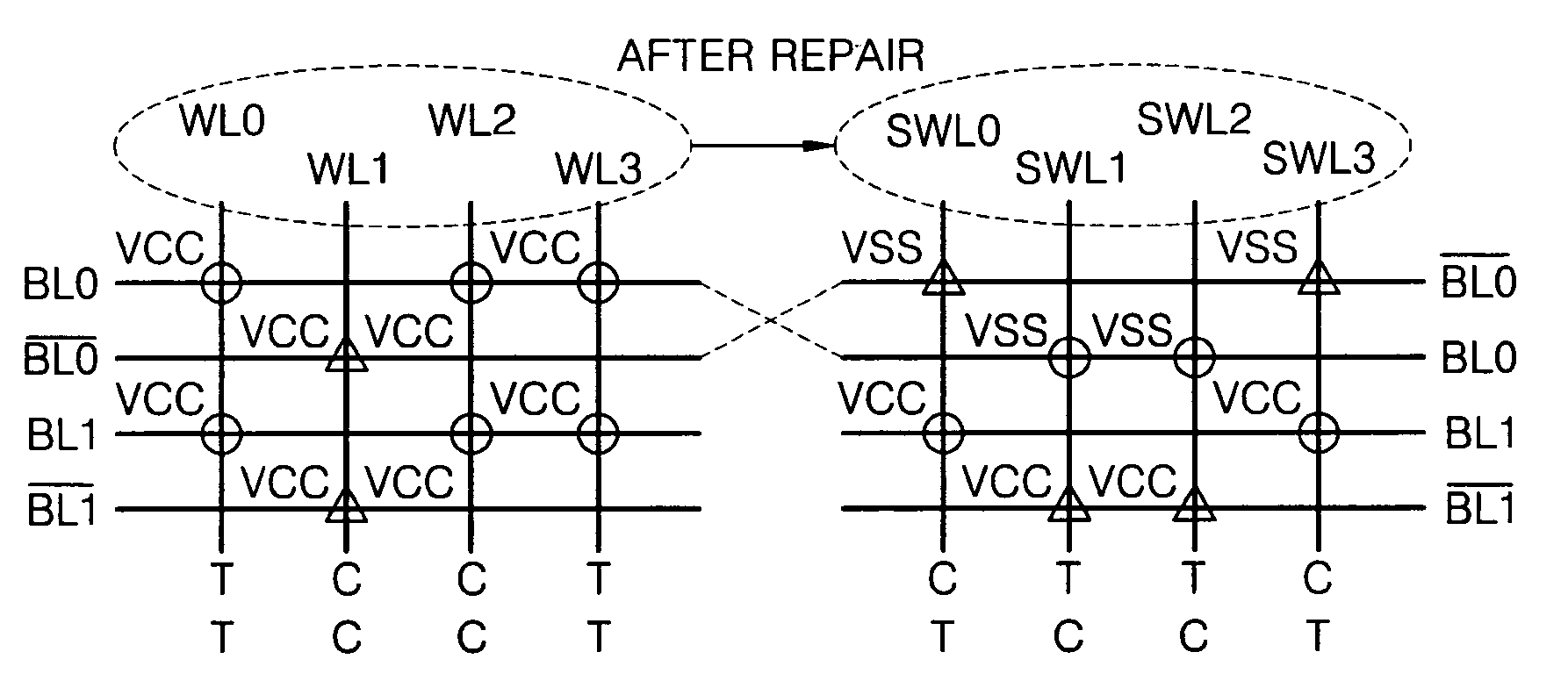
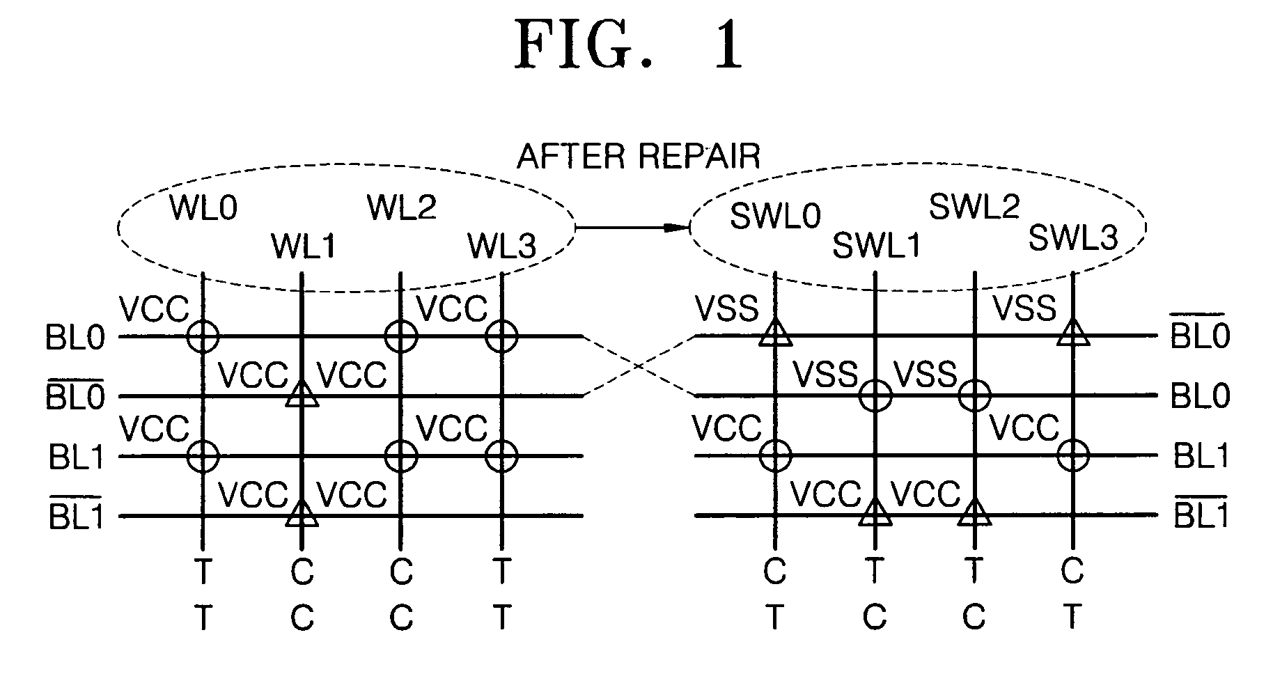
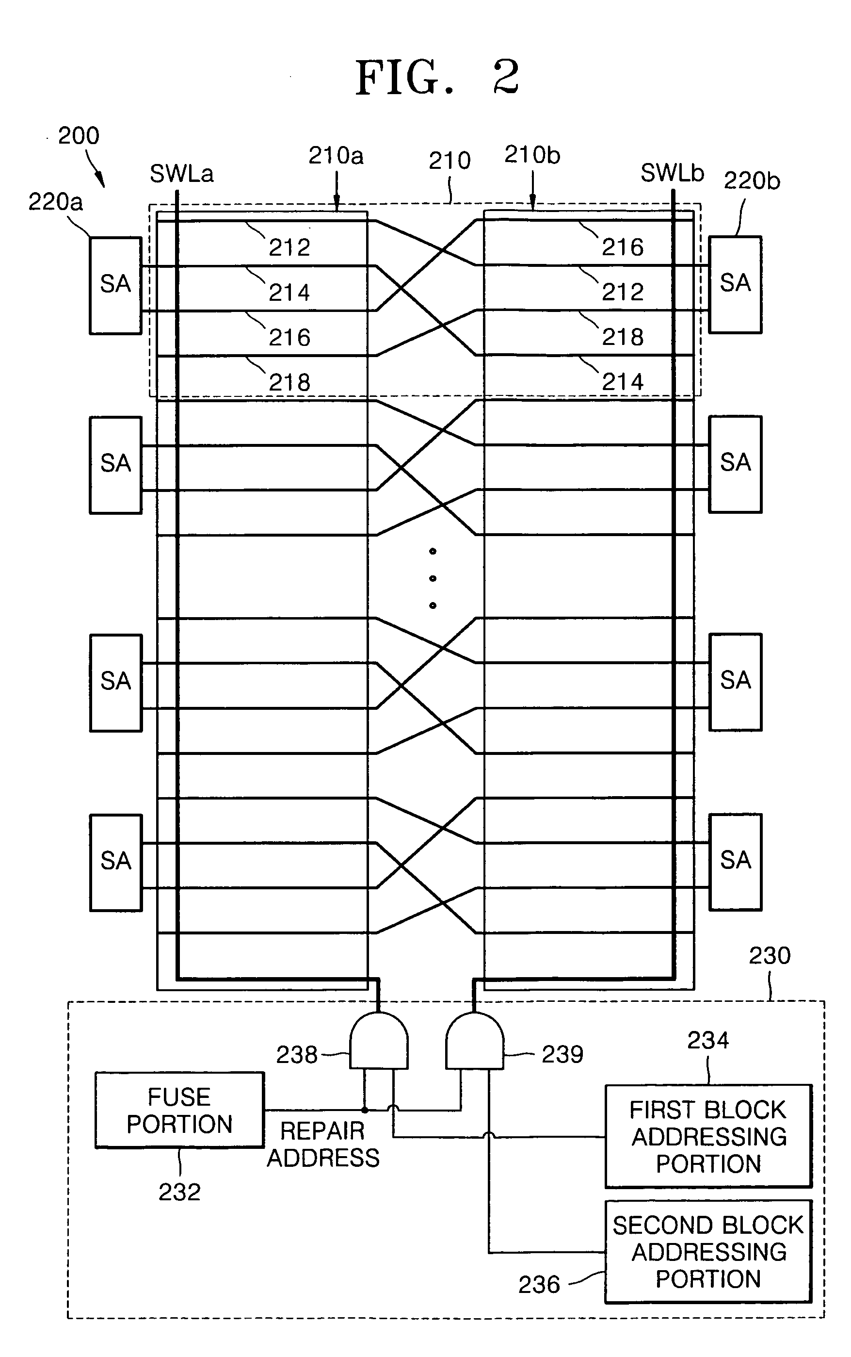
[0027] The invention is described more fully hereinafter with reference to the accompanying drawings, in which embodiments of the invention are shown. This invention may, however, be embodied in many different forms and should not be construed as limited to the embodiments set forth herein. Rather, these embodiments are provided so that this disclosure will be thorough and complete, and will fully convey the scope of the invention to those skilled in the art. In the drawings, the size and relative sizes of layers and regions may be exaggerated for clarity.

[0028] It will be understood that when an element or layer is referred to as being “on”, “connected to” or “coupled to” another element or layer, it can be directly on, connected or coupled to the other element or layer or intervening elements or layers may be present. In contrast, when an element is referred to as being “directly on,”“directly connected to” or “directly coupled to” another element or layer, there are no interveni...


PUM


Abstract

Redundancy circuits are provided for an integrated circuit memory device including a first memory cell block including a plurality of primary wordlines and a spare wordline, each associated with a plurality of memory cells; a second memory cell block including a plurality of primary wordlines and a spare wordline, each associated with a plurality of memory cells; and a plurality of bitlines extending across both the first and the second memory cell blocks the plurality of bitlines having a twisted bitline structure in which the bitlines are twisted between the first memory cell block and the second memory cell block and are not twisted within the respective memory cell blocks. The redundancy circuit is coupled to the primary and spare wordlines of both the first memory cell block and the second memory cell block. The redundancy circuit is also configured to select the spare wordline of the first memory cell block to replace one of the primary wordlines of the first memory cell block associated with a defective cell and to select the spare wordline of the second memory cell block to replace one of the primary wordlines of the second memory cell block associated with a defective cell so that data stored in spare cells connected to a selected spare wordline have a same data scramble as that of cells connected to the correspond.

Description

CROSS-REFERENCE TO RELATED APPLICATION [0001] This application claims the priority of Korean Patent Application No. 2004-42911, filed on Jun. 11, 2004, the disclosure of which is hereby incorporated herein by reference in its entirety. BACKGROUND OF THE INVENTION [0002] The present invention relates to integrated circuit devices and, more particularly, to redundancy circuits for memory devices and methods of repairing defective cells. [0003] As the cell density of semiconductor memory devices, such as dynamic random access memories (DRAMs), increases, the interval between bitlines thereof generally decreases. As a result, bitline coupling noise may be significantly increased during sensing of memory cell data. A twist bitline scheme has been proposed to reduce bitline coupling noise. [0004] In the twist bitline design, a bitline BL and a complementary bitline {overscore (BL)} are typically twisted at regular intervals. By adequately controlling the layout arrangement between an odd ...

Claims


Application Information

Patent Timeline
IPC IPC(8): H01L21/8242G11C7/18G11C8/00G11C11/22G11C11/401G11C11/4063G11C11/4097G11C29/00G11C29/04H01L27/108
CPCG11C7/18G11C29/816G11C11/4097G11C11/401G11C8/14G11C29/787
Inventor MIN, YOUNG-SUNKIM, NAM-JONG
Owner SAMSUNG ELECTRONICS CO LTD
Features
  • R&D
  • Intellectual Property
  • Life Sciences
  • Materials
  • Tech Scout
  • Unparalleled Data Quality
  • Higher Quality Content
  • 60% Fewer Hallucinations
Learn More