
Timing analysis method and apparatus

a timing analysis and time-based technology, applied in the field of timing analysis methods and apparatuses, can solve the problems of difficult to determine the appropriate design margin, inability to take into account the variation of the intra-chip, etc., and achieve the effect of realistic and highly accurate timing design

Active Publication Date: 2005-12-15
PANASONIC SEMICON SOLUTIONS CO LTD
View PDF18 Cites 13 Cited by
  • Summary
  • Abstract
  • Description
  • Claims
  • Application Information

AI Technical Summary

Benefits of technology

[0028] In this method, the design margin of each signal path can be corrected in accordance with the degree of variation different depending upon the number of stages or the like of circuit cells included therein, and hence, a delay excluding an excessive margin can be obtained.
[0030] Furthermore, when a relationship between a logic depth and an extent of averaging of delay variation of each of the signal paths is previously obtained and the corrected design margin is obtained by using the relationship, the timing analysis can be performed more rapidly.
[0036] In this method, when an apparatus for the correction is added to a conventional timing analysis apparatus, the design margin of each signal path can be corrected in accordance with the degree of variation different depending upon the number of stages of circuit cells or the like of each signal path, and therefore, a delay excluding an excessive margin can be more inexpensively obtained.
[0038] Thus, the design margin of each signal path can be corrected in accordance with the degree of variation different depending upon the number of stages of circuit cells or the like of each signal path, and therefore, a delay excluding an excessive margin can be obtained.
[0039] As described so far, in the timing analysis method or the timing analysis apparatus for an LSI according to this invention, a design margin can be set in consideration of the characteristics of each signal path with a plurality of differently behaving fabrication variation components superimposed. Accordingly, more realistic and highly accurate timing design can be performed on a large-scale circuit.
[0040] Moreover, a design margin can be set in consideration of a variation factor other than fabrication variation in a labor-saving manner, and hence, more realistic and highly accurate timing design can be performed on a large-scale circuit.

Problems solved by technology

However, the intra-chip variation component is not the variation caused when the circuit cells are similarly varied but the variation caused when the circuit cells are indiscriminately, namely, randomly, varied and therefore, the intra-chip variation cannot be taken into consideration by using the simple sum of the worst delays.
Actually, both the intra-chip variation component and the extra-chip variation component mixedly affect the circuit characteristics, and hence, it is not easy to determine an appropriate design margin.

Method used


Image

  • Timing analysis method and apparatus
  • Timing analysis method and apparatus
  • Timing analysis method and apparatus

Examples


embodiment 1

[0073] Now, a timing analysis apparatus for an LSI according to Embodiment 1 of the invention in which fabrication variation is taken into consideration will be described with reference to the accompanying drawings.

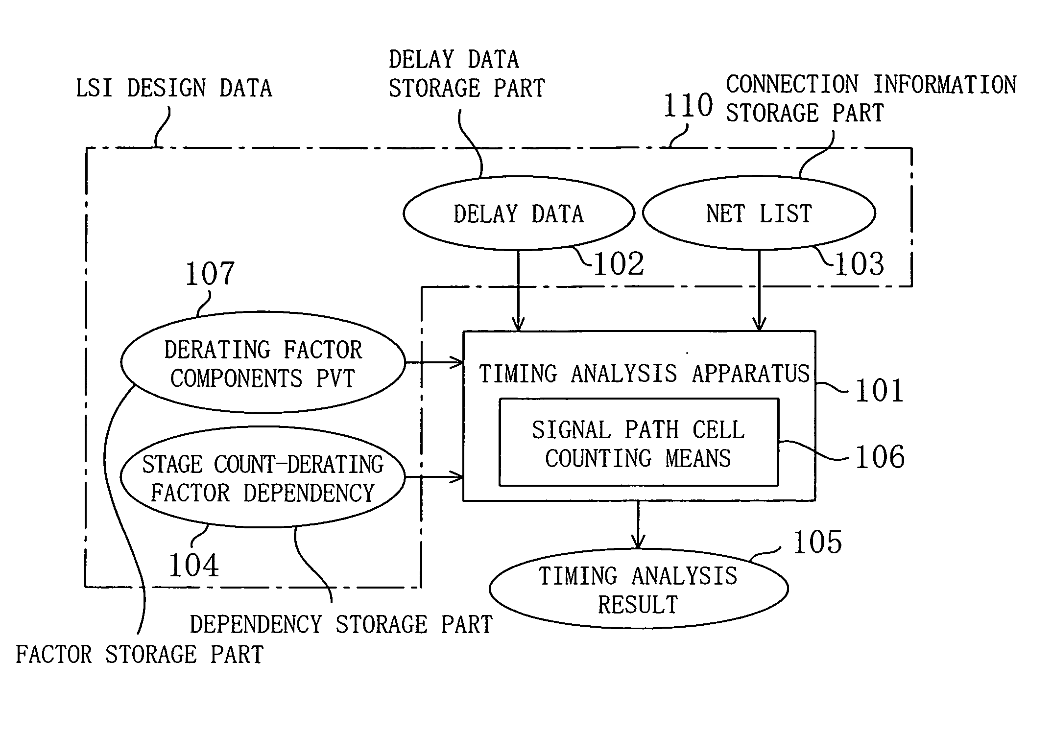
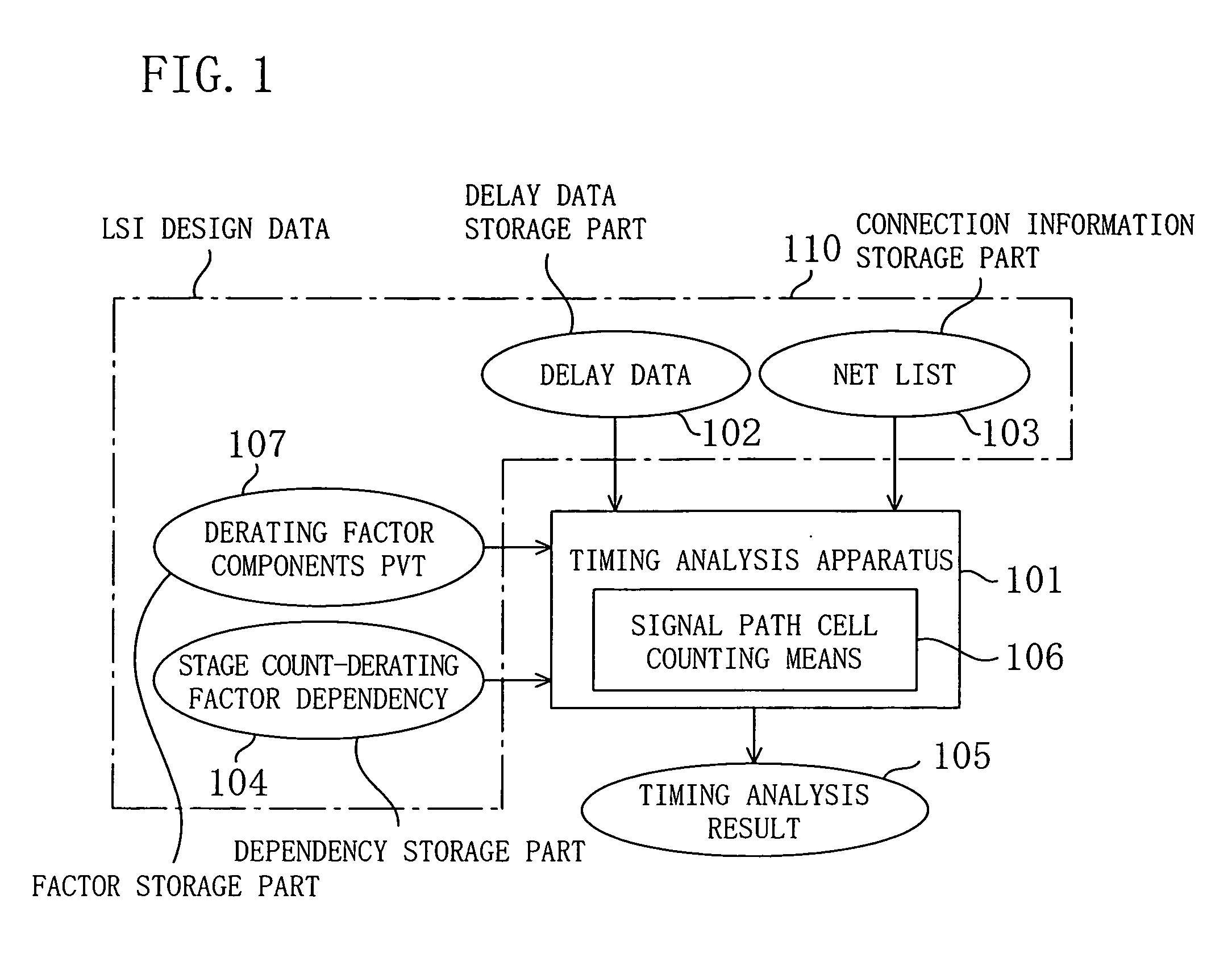
[0074]FIG. 1 is a block diagram for showing the architecture of a system used for performing the timing analysis for an LSI according to Embodiment 1 of the invention. As shown in FIG. 1, a timing analysis apparatus 101 performs the timing analysis on the basis of information supplied from respective information storage parts of LSI design data 110 in which information on the LSI is comprehensively stored. The LSI design data 110 includes a connection information storage part for storing a net list 103 describing connection information and the like of circuit cells included in the LSI; a delay information storage part for previously storing delay data 102 describing delay information of the circuit cells; a dependency storage part for storing stage count-derating factor ...

embodiment 2

[0142] Now, a timing analysis apparatus for an LSI according to Embodiment 2 of the invention in which the fabrication variation is taken into consideration will be described with reference to the accompanying drawings. Herein, redundant parts described in Embodiment 1 will be omitted. Also in this embodiment, the computer system shown in FIG. 2 is used for the timing analysis.

[0143]FIG. 21 is a block diagram for showing the architecture of a system used for performing the timing analysis for an LSI according to Embodiment 2. As shown in FIG. 21, first and second timing analysis parts 120 and 122 perform the timing analysis on the basis of information supplied from respective information storage parts of LSI design data 110 comprehensively storing information of the LSI. Similarly to Embodiment 1, the LSI design data 110 includes a connection information storage part for storing a net list 103 describing connection information and the like of circuit cells included in the LSI; a de...

embodiment 3

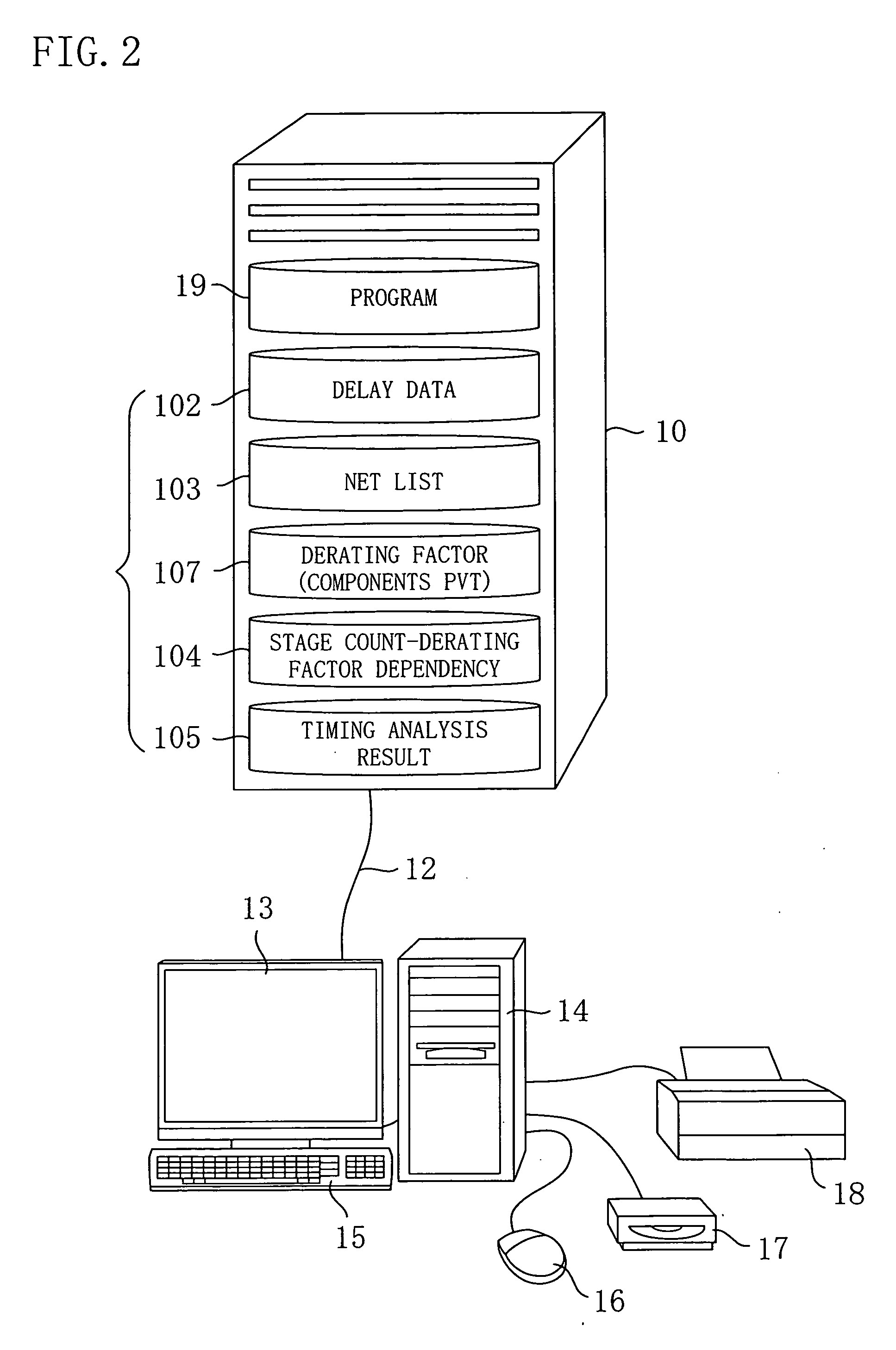
[0161] Now, a timing analysis apparatus for an LSI according to Embodiment 3 of the invention in which the non-fabrication variation is taken into consideration will be described with reference to the accompanying drawings. Herein, redundant parts described in Embodiment 1 will be omitted. Also in this embodiment, the timing analysis apparatus 101 shown in FIG. 1 and the computer system shown in FIG. 2 are used for the timing analysis, which is performed in accordance with the flowchart of FIG. 4 as follows:

[0162]—Signal Path Cell Counting Step—

[0163] The timing analysis apparatus 101 reads the net list 103 including the connection information and the like of circuit cells included in the LSI and the delay data 102 previously storing delay information of the circuit cells. The net list 103 stores the connection information and the like of the circuit cells included in the circuit subjected to the timing analysis. The delay data 102 stores information of a delay time of each stage (...


PUM


Abstract

A timing analysis apparatus reads a net list including connection information and the like of circuit cells of an LSI, delay data for previously storing delay information of the circuit cells, stage count-derating factor dependency and components P, V and T of a derating factor; detects the number of stages of each signal path by a signal path cell counting section; determines a derating factor corresponding to the extent of averaging of random variation of each signal path in accordance with the number of stages of the signal path; and performs timing analysis on the basis of the determined derating factor. Therefore, more realistic and highly accurate timing design can be performed on a large-scale circuit.

Description

CROSS-REFERENCE TO RELATED APPLICATIONS [0001] This application claims priority under 35 U.S.C. §119 on Patent Application No. 2004-173113 filed in Japan on Jun. 10, 2004, the entire contents of which are hereby incorporated by reference. BACKGROUND OF THE INVENTION [0002] The present invention relates to a technique employed in design of a system LSI, an ASIC (application specific IC) or the like for performing timing analysis with a design margin set in consideration of influence of variation mainly caused in fabrication. [0003] Recently, refinement and the degree of integration of transistors have been rapidly improved in accordance with the development of fabrication technique, and a variety of functions can be now realized on one chip of a CMIS (complementary metal insulator semiconductor) integrated circuit (hereinafter referred to as the LSI). In developing such an LSI, a design margin is generally provided. There are various factors affecting circuit characteristics, and a d...

Claims


Application Information

Patent Timeline
IPC IPC(8): G06F17/50G11C7/00H01L21/82
CPCG06F17/5031G06F30/3312
Inventor YONEZAWA, HIROKAZU
Owner PANASONIC SEMICON SOLUTIONS CO LTD
Learn More