Low temperature epitaxial growth of silicon-containing films using UV radiation
a technology of epitaxial growth and silicon-containing films, which is applied in the testing/measurement of individual semiconductor devices, semiconductor/solid-state devices, semiconductor devices, etc., can solve the problems of low recombinative hcl desorption rate, low equipment cost, and decrease in film growth rate, so as to increase the adsorption rate of precursor materials, enhance surface reaction, and high quality
- Summary
- Abstract
- Description
- Claims
- Application Information
AI Technical Summary
Benefits of technology
Problems solved by technology
Method used
Image

Examples
example one
[0061] Prior to epitaxial growth of a silicon-containing film on a substrate, it is necessary to remove native oxides on the substrate surface which affect the surface lattice structure, and to terminate dangling bonds with hydrogen, to provide a clean passivated surface for subsequent growth of a silicon-containing epi film. Often, the substrate is a silicon wafer having a native oxide on the wafer surface. The bulk of the native oxide is removed using a wet chemical process, typically an aqueous HF dip. Subsequent to this bulk removal of native oxides, we used an in-situ cleaning / passivation process carried out in the coating deposition chamber to remove residual oxide and hydrocarbon and to passivate the substrate surface prior to epitaxial growth of the silicon-containing film. During the in-situ cleaning / passivation method the substrate is exposed to a hydrogen ambient in the processing volume with simultaneous exposure to radiation at a wavelength of about 180 nm or lower. In ...
example two
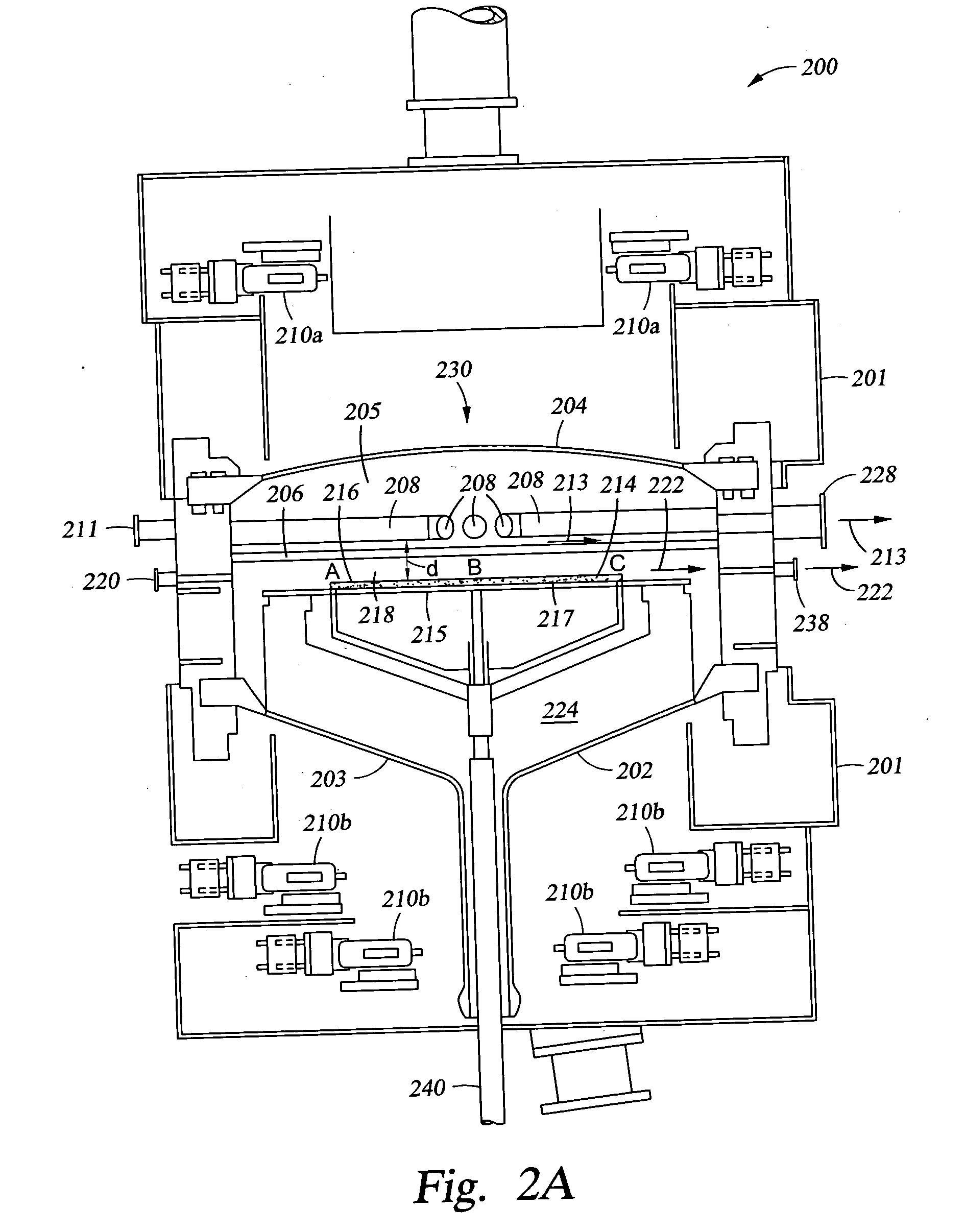
[0062]FIG. 3A shows a graph 300 of the epitaxial growth rate of a silicon / germanium film with and without the benefit of 172 nm radiation within the film deposition process volume, for films deposited at temperatures ranging from 550° C. to 750° C. The substrate temperature in degrees C. is shown on scale 302, while the growth rate in Å / min is shown on scale 304. Curve 308 is representative of the film growth rate without the benefit of the 172 nm radiation. Curve 306 is representative of the film growth rate with the benefit of the 172 nm radiation. When the 172 nm radiation was present, the power density at the substrate surface was about 2 mW / cm2. The silicon-containing component of the deposition process gas was SiH2Cl2 and the germanium-containing component was GeH4, the ratio of silicon:germanium was in the range of about 1:20. The spacing “d” between the upper surface 216 of substrate 214 and the radiation sources 208 (as shown in FIG. 2A) quartz window 206 and the substrate ...
example three
[0063]FIG. 4 shows a graph 400 of the enhancement of growth rate of a silicon / germanium film due to the employment of the 172 nm radiation in the process volume during film formation. The growth rate is shown as a function of the substrate temperature at which the film growth is carried out. The process conditions were those described above with reference to FIG. 3. The substrate temperature is shown in degrees C. on scale 402, the increase in growth rate of the silicon / germanium film is shown on scale 404, and Curve 406 shows the relationship, which illustrates that the presence of the 172 nm radiation in the process volume has an increasing beneficial effect at lower temperatures.
PUM
| Property | Measurement | Unit |
|---|---|---|
| Temperature | aaaaa | aaaaa |
| Temperature | aaaaa | aaaaa |
| Temperature | aaaaa | aaaaa |
Abstract
Description
Claims
Application Information
 - R&D Engineer
- R&D Manager
- IP Professional
- Industry Leading Data Capabilities
- Powerful AI technology
- Patent DNA Extraction
Browse by: Latest US Patents, China's latest patents, Technical Efficacy Thesaurus, Application Domain, Technology Topic.
© 2024 PatSnap. All rights reserved.Legal|Privacy policy|Modern Slavery Act Transparency Statement|Sitemap