Display device and method of driving the same

a display device and drive technology, applied in static indicating devices, instruments, electroluminescent light sources, etc., can solve the problems of difficult to achieve the improvement of the aperture ratio of each pixel, the inability to realize large high-resolution display devices, and the inability to achieve the improvement of the aperture ratio. , to achieve the effect of suppressing the deterioration of the display image quality and suppressing the gate-to-source voltag

Active Publication Date: 2005-12-22
INNOLUX CORP
View PDF6 Cites 39 Cited by
  • Summary
  • Abstract
  • Description
  • Claims
  • Application Information

AI Technical Summary

Benefits of technology

[0014] The display and the method of driving the display according to the present invention allows the downsizing of the interconnection structure which serves to transmit the electric signals to the pixel circuit to determine the start timing and the end timing of each process. Specifically, according to the display and the method of driving the display according to the present invention, the same start timing of the electric charge accumulation and the same start timing of the voltage detection / supply corresponding to the threshold voltage are set for the pixel circuits arranged in the first row and the second row, and the same end timing of the electric charge accumulation and the same end timing of the voltage detection / supply corresponding to the threshold voltage are set for the pixel circuits arranged in the first row and the third row. In addition, when the timings are determined in the above-described manner, the variation in the time length required for the electric charge accumulation is same with the variation in the time length required for the voltage detection / supply in the pixel circuits in the adjacent row. Hence, the variation in the source potential of the transistor element caused by the increase or the decrease in the time length required for the electric charge accumulation is offset by the variation in the source potential of the transistor element caused by the increase or the decrease in the voltage detection / supply, whereby the variation in the gate-to-source voltage can be suppressed as a whole. Thus, according to the invention recited in claim 1, regardless of the reduction in the number of wirings supplying the electric signals to the pixel circuits, the variation in the gate-to-source voltage among the pixel circuits arranged in the different rows can be suppressed and the deterioration of the display image quality can be suppressed.

Problems solved by technology

The former, though being advantageous for its simple structure, is not appropriate for realization of large high-resolution display devices.
The conventional display device with the OLEDs, however, has a large number of wirings extending from the driver circuit 112 as an interconnection structure, whereby the improvement in aperture ratio of each pixel is difficult to achieve.
Thus, the interconnection structure occupies extremely large area on the array substrate.
Then the improvement in aperture ratio is difficult to achieve.
However, such structure creates another problem, i.e., the level of the driving threshold voltage supplied by the driver element 102 fluctuates, for example, to deteriorate the display image quality.

Method used


Image

  • Display device and method of driving the same
  • Display device and method of driving the same
  • Display device and method of driving the same

Examples


Embodiment Construction

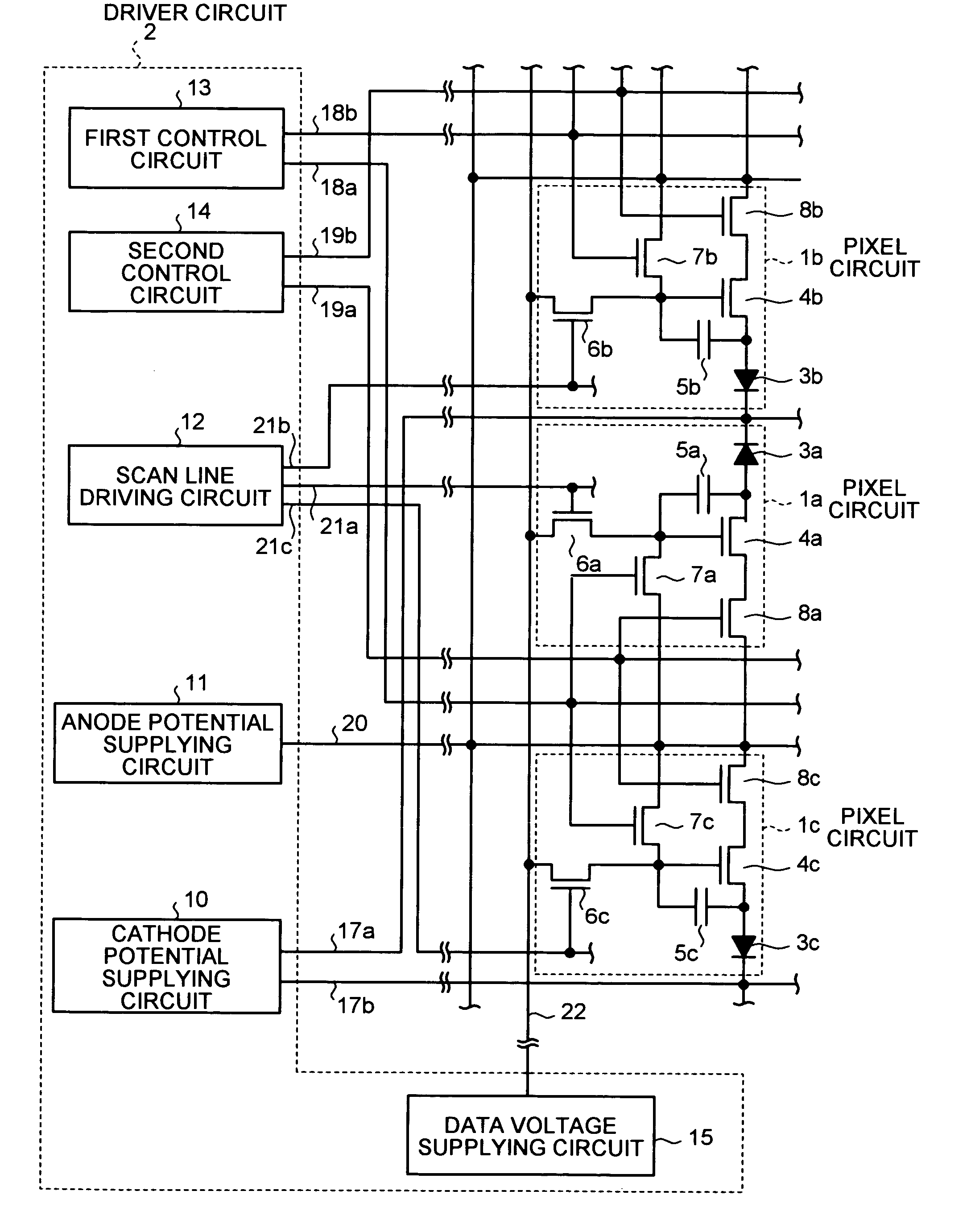
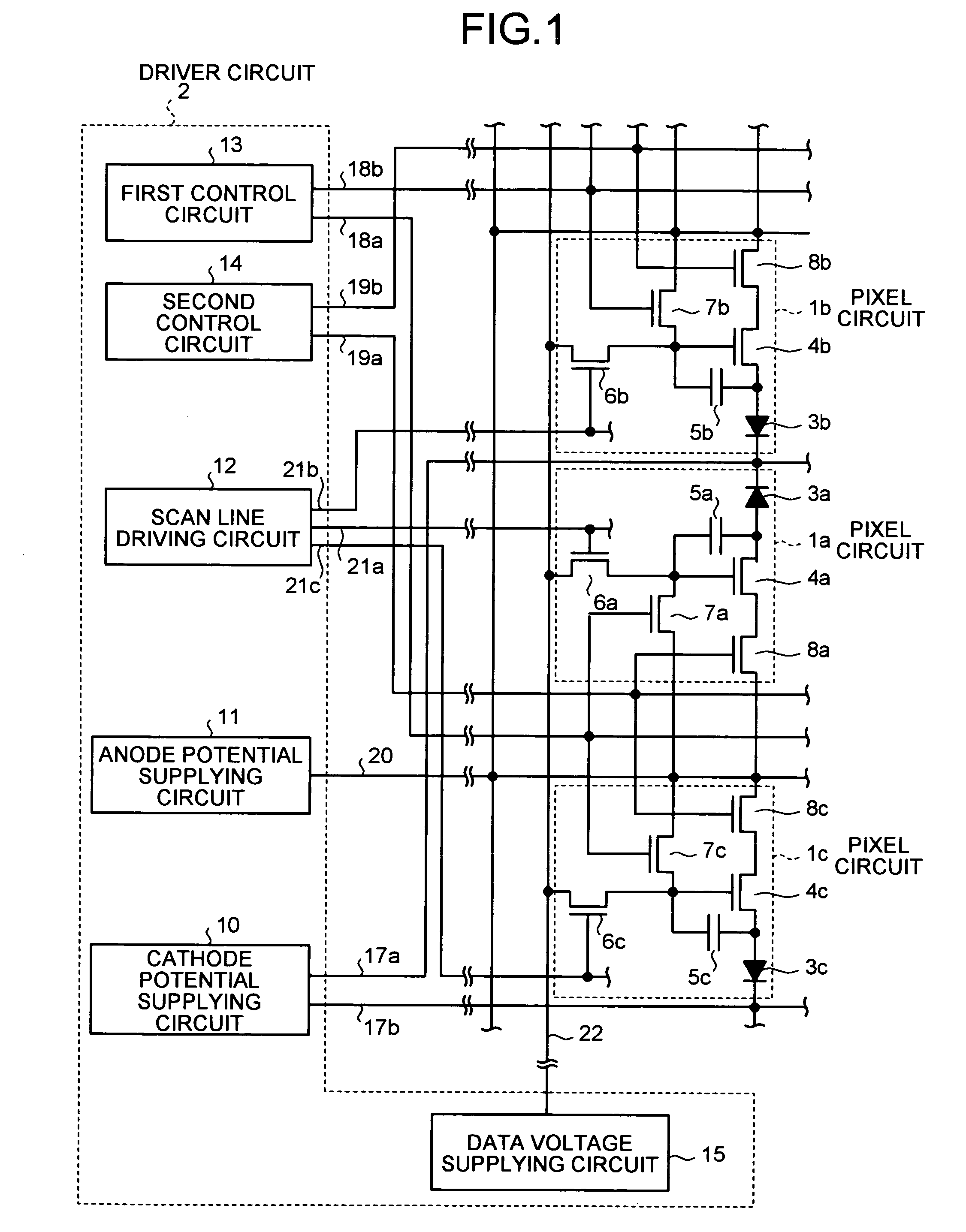
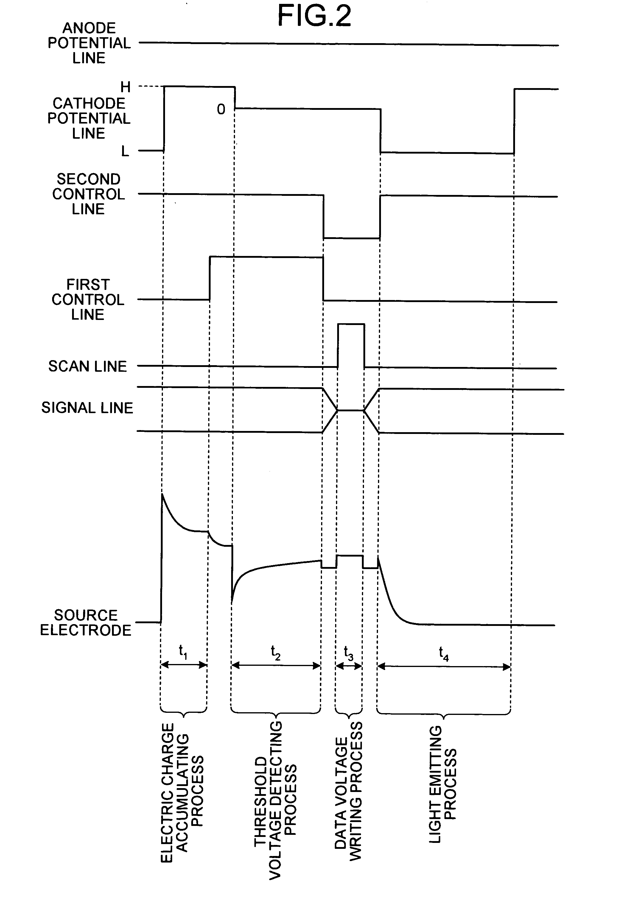
[0023] Exemplary preferred embodiments (hereinafter simply referred to as embodiments) of a display device according to the present invention will be described below with reference to the drawings. It should be noted that the drawings are exemplary only and may be different from an actual structure, and may be different in dimension or proportion with each other. Though an n-channel thin film transistor will be described as a component of the embodiment, a p-channel transistor of course is adoptable for the present invention. Further in the following description, when electrodes other than a gate electrode of the thin film transistor are functionable either as a source electrode or a drain electrode, such structure is referred to as a source / drain electrode.

[0024] A display device according to the embodiment includes pixel circuits arranged as a matrix. Plural pixel circuits arranged in different rows share a part of interconnection structure which supplies electric signals. Throug...


PUM


Abstract

A display device includes a driver circuit that controls so that an electric charge accumulation and a voltage detection / supply start simultaneously for a pixel circuit in a first row in the matrix and a pixel circuit in a second row in a matrix and adjacent to the pixel circuit in the first row in one direction along a column, and that controls so that the electric charge accumulation and the voltage detection / supply end simultaneously for the pixel circuit in the first row and a pixel circuit in a third row and adjacent to the pixel circuit in the first row in another direction along the column.

Description

BACKGROUND OF THE INVENTION [0001] 1. Field of the Invention [0002] The present invention relates to a display device including plural pixel circuits arranged in a matrix, each pixel circuit having a light-emitting element that emits light with a luminance corresponding to an amount of injected electric current and a transistor element that controls the amount of electric current flowing through the light-emitting element, the display device being formed to accumulate electric charges up to a predetermined capacitor and to detect / supply a voltage corresponding to a driving threshold voltage between a gate and a source of the transistor using the accumulated electric charges prior to the light emission by the light-emitting element. The present invention also relates to a method of driving such display device. [0003] 2. Description of the Related Art [0004] An organic light-emitting display device which employs an organic light-emitting diode (OLED) that emits light by itself is the ...

Claims


Application Information

Patent Timeline
Patent Type & Authority Applications(United States)
IPC IPC(8): G09G3/30H05B44/00
CPCG09G3/3233G09G3/3291G09G2300/0426G09G2300/0465G09G2330/02G09G2300/0842G09G2310/0256G09G2310/0262G09G2310/08G09G2300/0819
Inventor MIWA, KOHICHIONO, SHINYAKOBAYASHI, YOSHINAO
Owner INNOLUX CORP
Why Eureka
Try Eureka