
Printed circuit boards having improved solder pads

Inactive Publication Date: 2005-12-22
HON HAI PRECISION IND CO LTD
View PDF3 Cites 1 Cited by
  • Summary
  • Abstract
  • Description
  • Claims
  • Application Information

AI Technical Summary

Benefits of technology

[0008] An object of the present invention is to provide a printed circuit board that has improved solder pad layout for preventing short circuit of the printed circuit board.

Problems solved by technology

This insertion process is unduly laborious and time-consuming and has a low efficiency.
But the axial leads are often bent when the components are inserted into the through holes by machine.
When the axial lead of the component is out of the area of the soldering pad, it is prone to touch the circuit that surrounds the soldering pad.
Thus a short circuit in the printed circuit board occurs and this causes damage to the printed circuit board.

Method used


Image

  • Printed circuit boards having improved solder pads
  • Printed circuit boards having improved solder pads
  • Printed circuit boards having improved solder pads

Examples


Embodiment Construction

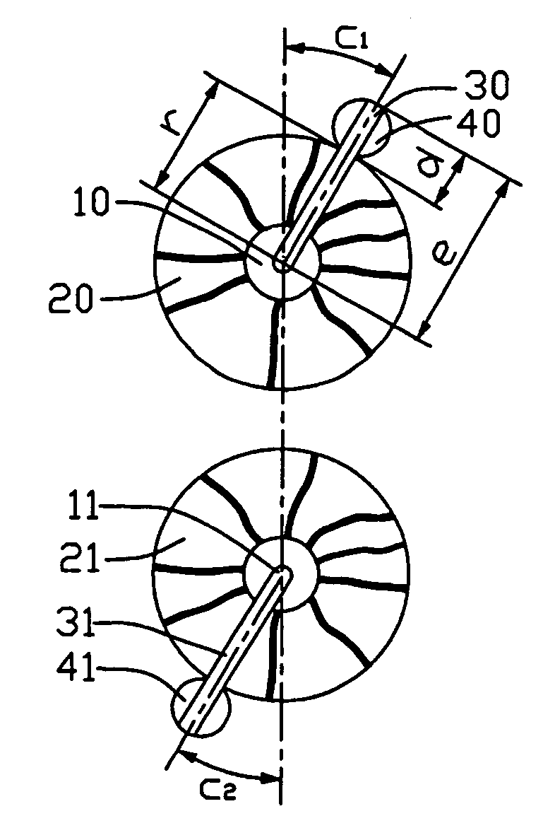
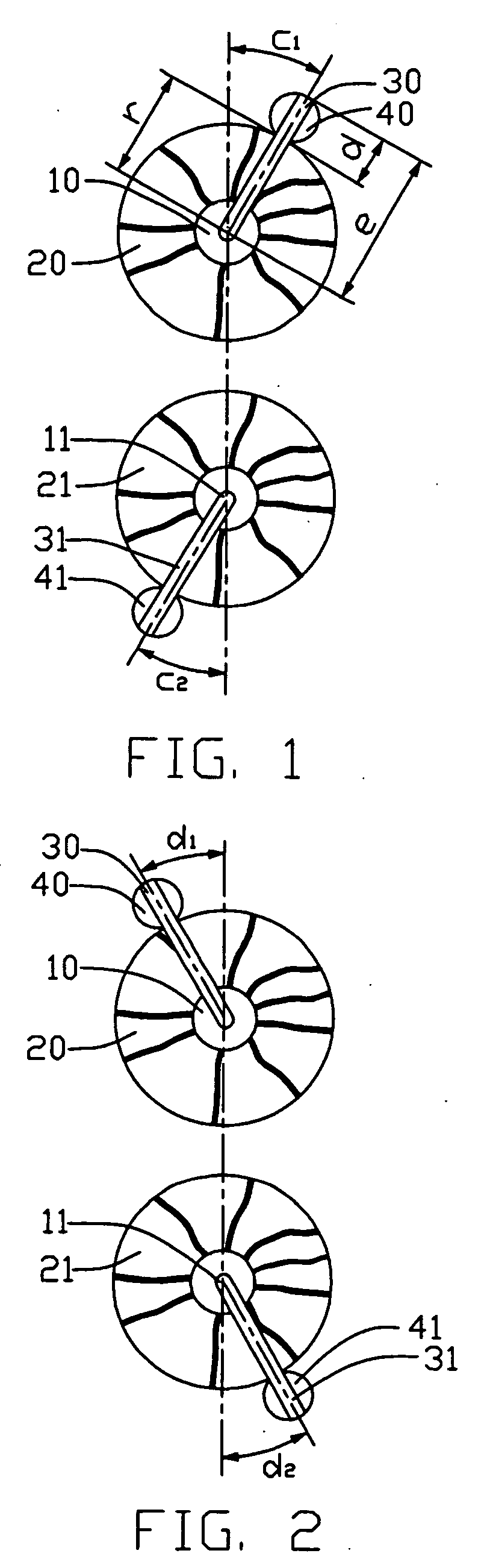
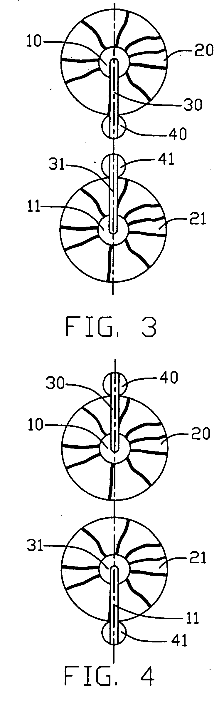
[0013] FIGS. 1 to 4 illustrate a pair of solder pads in accordance with the present invention. A pair of plated through holes 10, 12 which may be arranged in a row is provided to receive conventional components such as a resistor which has axial leads 30, 31 formed therefrom to project through holes 10, 12. The components are electrically and physically connected to the printed circuit board by passing the entire printed circuit board through a wave soldering operation. A pair of first pads 20, 21 are located on a same surface of the printed circuit board and respectively around the through holes 10, 11. The first pads 20, 21 are covered with solder. A pair of second pads 40, 41 are circular and covered with the same solder of the first pads 20, 21. A plurality solder pads such as the first pads 20, 21 and the second pads 40, 41 are disposed on the printed circuit board. The solder pads have no circuits disposed thereon and are for preventing from short circuit between neighboring c...


PUM


Abstract

A printed circuit board having improved solder pads for preventing from short circuit of the printed circuit board caused by axial leads (30, 31) of components engaging the circuit surrounding the soldering pad comprises a pair of through holes (10, 11), a pair of first pads (20, 21) surrounding corresponding through holes and a pair of second pads (40, 41) adjacent corresponding first pads. When components are inserted into the through holes of the printed circuit board using placement machines, bent portions of the axial leads that are extended out of the first pads will fall into the second pads.

Description

BACKGROUND OF THE INVENTION [0001] 1. Field of the Invention [0002] The present invention relates to a printed circuit board, and particularly to a printed circuit board which has improved solder pads layout. [0003] 2. Description of Related Art [0004] Conventional printed circuit boards each define a plurality of through holes. The through holes are provided for extension of leads of components. The components are connected with the printed circuit board with the leads soldered thereto. A solder pad area is provided around each through hole when layout. Circuit is not laid in the pad areas and the pad areas are commonly covered with solder. The components are attached to the printed circuit board by wave soldering or reflow soldering. The pad areas are for preventing short circuit between the components and the circuit around the components on the printed circuit board. [0005] Bigger components with axial leads are typically inserted into the printed circuit board manually. This in...

Claims


Application Information

Patent Timeline
IPC IPC(8): H01R12/00H05K1/11H05K3/34
CPCH05K1/116H05K3/3447H05K2203/1446H05K2201/09781H05K2201/10651H05K2201/0949
Inventor WANG, PINGLI, YAN-FANG
Owner HON HAI PRECISION IND CO LTD
Features
  • Generate Ideas
  • Intellectual Property
  • Life Sciences
  • Materials
  • Tech Scout
  • Unparalleled Data Quality
  • Higher Quality Content
  • 60% Fewer Hallucinations
Learn More