Microelectronic packages and methods therefor

Active Publication Date: 2005-12-29
TESSERA INC
View PDF33 Cites 231 Cited by
  • Summary
  • Abstract
  • Description
  • Claims
  • Application Information

AI Technical Summary

Benefits of technology

[0020] In certain preferred embodiments, the conductive posts are movable independently of one another, and are movable relative to the microelectronic element. The independent movement of the conductive posts enables the posts to conform to a non-planar surface of a second microelectronic element so as to form a reliable electrical interconnection between the package and the second microelectronic element.
[0033] In still other preferred embodiments of the present invention, a microelectronic assembly includes at least two stacked microelectronic packages. Each microelectronic package desirably includes a microelectronic element, a flexible substrate having a top surface and a bottom surface, the substrate overlying and being spaced from a face of the microelectronic element, and a plurality of conductive posts exposed at a bottom surface of the flexible substrate, the conductive posts being electrically interconnected with the microelectronic element. The at least two stacked microelectronic packages desirably include a first microelectronic package and a second microelectronic package stacked atop the first microelectronic package so that the conductive terminals of the second microelectronic package confront the top surface of the flexible substrate of the first microelectronic package. The assembly also desirably includes a rigid conductive material connecting ends of the conductive terminals of the second microelectronic package with the flexible substrate of the first microelectronic package, whereby the rigid material prevents movement of the ends of the conductive terminals of the second microelectronic package.

Problems solved by technology

Assemblies including packages can suffer from stresses imposed by differential thermal expansion and contraction of the device and the substrate.
Where the terminals of the package are fixed relative to the chip or other device, these effects tend to cause the terminals to move relative to the contact pads on the circuit board.
This can impose stresses in the solder, which connects the terminals to the substrates.
Testing of packaged devices poses another formidable problem.
However, it is difficult to make connections by pressing the package against a simple test fixture such as an ordinary circuit board having planar pads.
For example, in a BGA package, differences in diameter of the solder balls attached to the terminals, and non-planarity of the chip carrier, may cause some of the solder balls to lie at different heights.
However, such features add to the cost of the test fixture and, in some cases, introduce some unreliability into the test fixture itself.
This is particularly undesirable because the test fixture, and the engagement of the device with the test fixture, should be more reliable than the packaged devices themselves in order to provide a meaningful test.
This requirement imposes constraints on the electrical characteristics of the signal paths in the test fixture, which further complicates construction of the test fixture.
Additionally, where the packaged device has solder balls on its terminals, solder tends to accumulate on those parts of the test fixture, which engage the solder balls.
This can shorten the life of the test fixture and impair its reliability.

Method used


Image

  • Microelectronic packages and methods therefor
  • Microelectronic packages and methods therefor
  • Microelectronic packages and methods therefor

Examples


Embodiment Construction

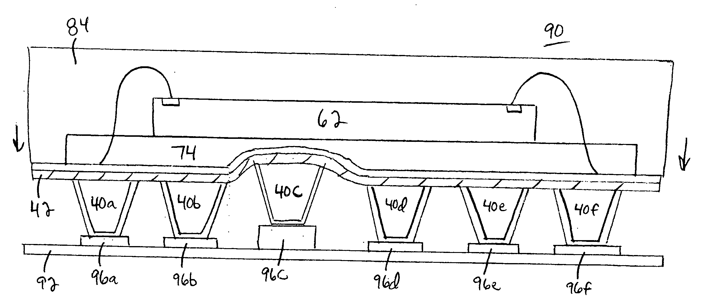
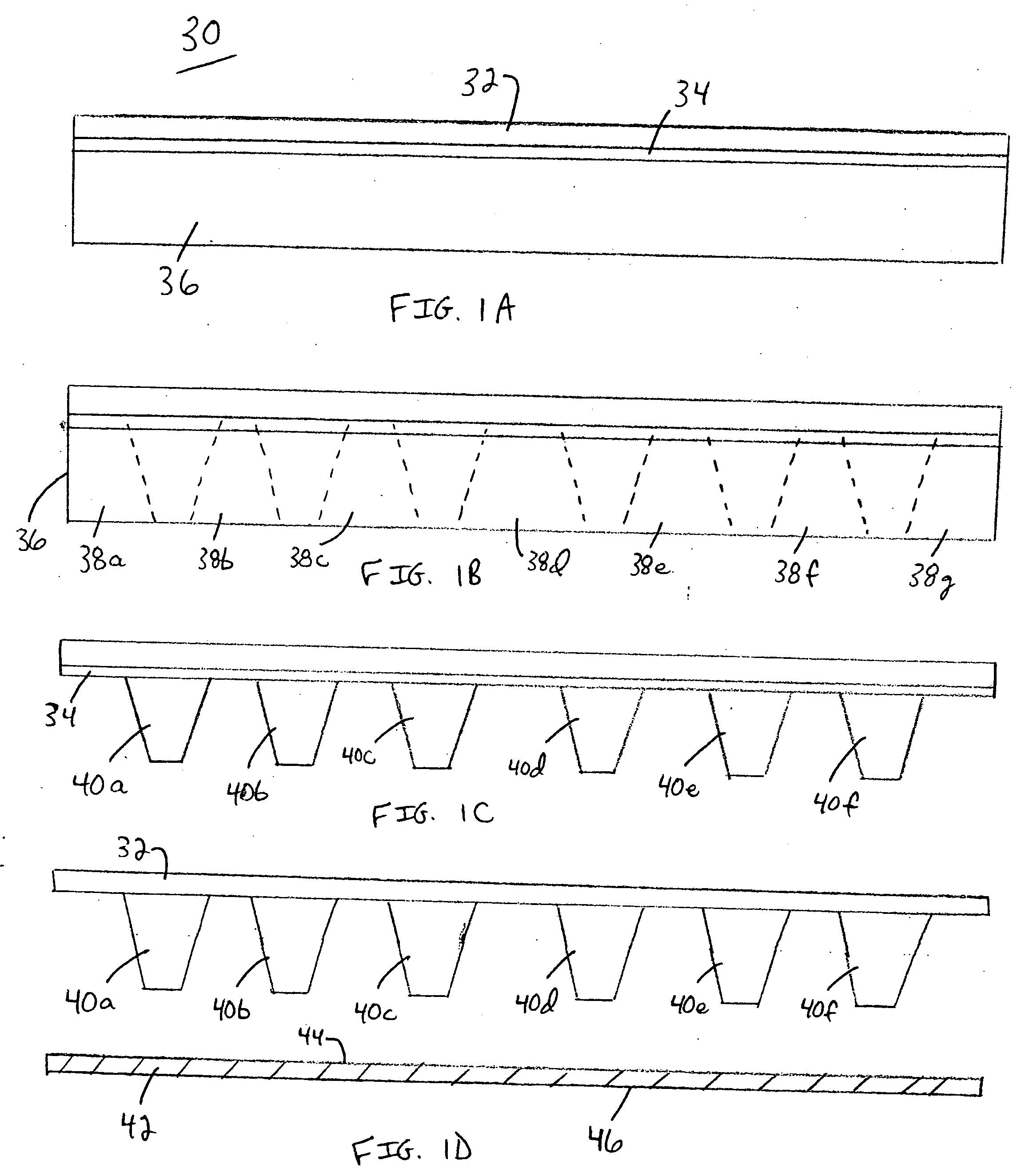
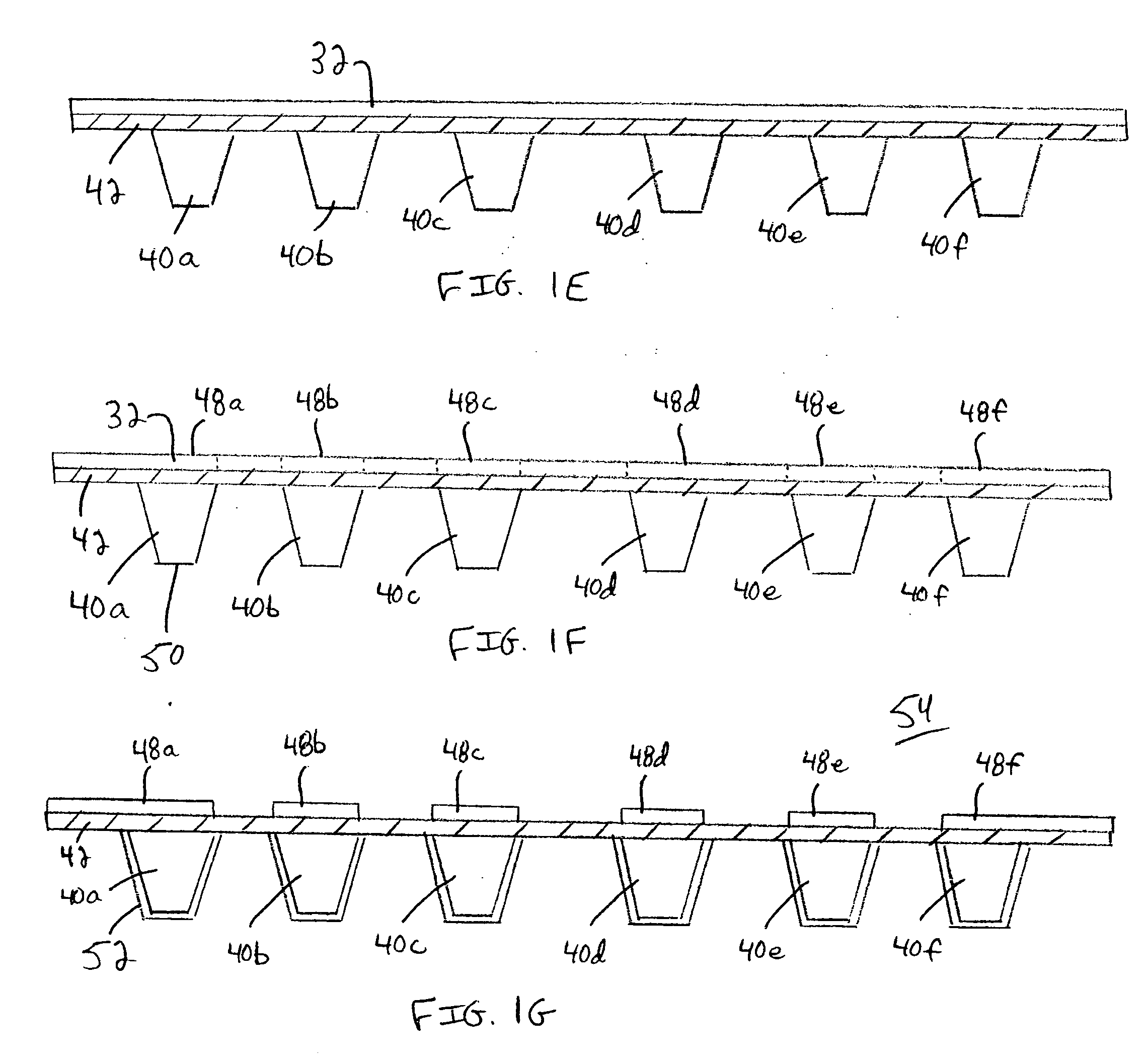
[0091] Referring to FIG. 1A, in certain preferred embodiments of the present invention, a microelectronic subassembly may be fabricated by a process such as that disclosed in certain preferred embodiments of co-pending, commonly assigned U.S. Provisional Application No. 60 / 508,970, the disclosure of which is incorporated by reference herein. As disclosed in certain preferred embodiments of the '970 application, a metallic plate 30 includes a top layer 32 made of a conductive material, an intermediate etch stop layer 34 and a bottom layer 36 made of a conductive material. The top and bottom layers 32, 36 may include electrically conductive materials such as copper. The intermediate etch stop layer 34 may include materials such as nickel. Referring to FIGS. 1B and 1C, the bottom layer 36 of metallic plate 30 is stamped or etched to remove portions 38a-38g of bottom layer 36 so as to form conductive terminals or posts 40a-40f. Referring to FIGS. 1C and 1D, after the posts 40a-40f have ...


PUM


Abstract

A microelectronic package includes a microelectronic element having faces, contacts and an outer perimeter, and a flexible substrate overlying and spaced from a first face of the microelectronic element, an outer region of the flexible substrate extending beyond the outer perimeter of the microelectronic element. The package includes a plurality of conductive posts exposed at a surface of the flexible substrate and being electrically interconnected with the microelectronic element, wherein at least one of the conductive posts is disposed in the outer region of the flexible substrate, and a compliant layer disposed between the first face of the microelectronic element and the flexible substrate, wherein the compliant layer overlies the at least one of the conductive posts that is disposed in the outer region of the flexible substrate. The package includes a support element in contact with the microelectronic element and the compliant layer, whereby the support element overlies the outer region of the flexible substrate.

Description

CROSS REFERENCE TO RELATED APPLICATIONS [0001] The present application claims benefit of U.S. Provisional Application Ser. Nos. 60 / 621,865, filed Oct. 25, 2004 and 60 / 583,066, filed Jun. 25, 2004, the disclosures of which are hereby incorporated by reference herein.FIELD OF THE INVENTION [0002] The present invention generally relates to microelectronic packages and more specifically to methods of making and testing microelectronic packages. BACKGROUND OF THE INVENTION [0003] Microelectronic devices such as semiconductor chips typically require many input and output connections to other electronic components. The input and output contacts of a semiconductor chip or other comparable device are generally disposed in grid-like patterns that substantially cover a surface of the device (commonly referred to as an “area array”) or in elongated rows which may extend parallel to and adjacent each edge of the device's front surface, or in the center of the front surface. Typically, devices su...

Claims


Application Information

Patent Timeline
IPC IPC(8): H01L23/02H01L23/31H01L23/367H01L23/498H01L25/10
CPCH01L23/3128H01L2924/3511H01L23/49811H01L23/4985H01L25/105H01L2224/16H01L2224/48091H01L2224/4824H01L2224/73204H01L2224/73265H01L2924/01004H01L2924/01078H01L2924/01079H01L2924/15311H01L2924/15312H01L2924/19041H01L23/3677H01L2225/1023H01L24/48H01L2224/32245H01L2224/48247H01L2224/32225H01L2224/16225H01L2225/1058H01L2924/00014H01L2924/00H01L2924/12042H01L2924/181H01L2924/00012H01L2224/45099H01L2224/45015H01L2924/207
Inventor HABA, BELGACEMBEROZ, MASUDKANG, TECK-GYUKUBOTA, YOICHIKRISHNAN, SRIDHARRILEY, JOHN B. IIIMOHAMMED, ILYAS
Owner TESSERA INC
Why Eureka
Try Eureka