High-density interconnecting adhesive tape

Active Publication Date: 2019-02-14
IBM CORP
View PDF5 Cites 6 Cited by
  • Summary
  • Abstract
  • Description
  • Claims
  • Application Information

AI Technical Summary

Benefits of technology

The present invention relates to an interconnection substrate and an electronic device made using this substrate. The substrate has an interconnection layer that allows signal transmission between chips through a defined area on the substrate. This interconnection layer includes an organic insulating material, which increases the density of interconnections while maintaining their reliability. As a result, the interconnection is more reliable with higher density. The electronic device fabricated using this substrate has a reliable interconnection with higher density.

Problems solved by technology

The silicon interposer technology requires an expensive BEOL (Back End Of Line) process to form high density circuitries on the silicon interposer and a TSV (Through Silicon Via) fabrication process to connect metallization layers on its front and back surfaces.
Also large insertion loss is caused by the TSV since the silicon into which the TSVs are fabricated is a semiconductor, not an insulator.
The EMIB (Embedded Multi-Die Interconnect Bridge) suffers from a problem of mechanical stress due to CTE (Coefficient for Thermal Expansion) mismatch between an organic substrate and a silicon bridge interconnect assembly embedded in the organic substrate, resulting in negative impacts on interconnection reliability and production yield.
The iTHOP requires an expensive chemical mechanical polishing (CMP) process as well as delicate fabrication processes to form high density interconnection layer over an organic build-up substrate.
The organic substrate on which the interconnection layer is fabricated is generally an unstable and warped substrate.

Method used


Image

  • High-density interconnecting adhesive tape
  • High-density interconnecting adhesive tape
  • High-density interconnecting adhesive tape

Examples


Embodiment Construction

[0060]Now, the present invention will be described using particular embodiments, and the embodiments described hereafter are understood to be only referred to as examples and are not intended to limit the scope of the present invention.

[0061]One or more embodiments according to the present invention are directed to an interconnection substrate, an electronic device including the interconnection substrate, an interconnection layer carrying structure used for fabrication of the interconnection substrate, a method for fabricating the interconnection substrate, a method for fabricating the electronic device and a method for fabricating the interconnection layer carrying structure, in which high density interconnections between chips mounted on the interconnection substrate are achieved in a novel manner.

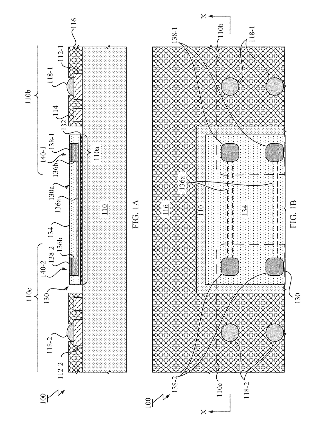
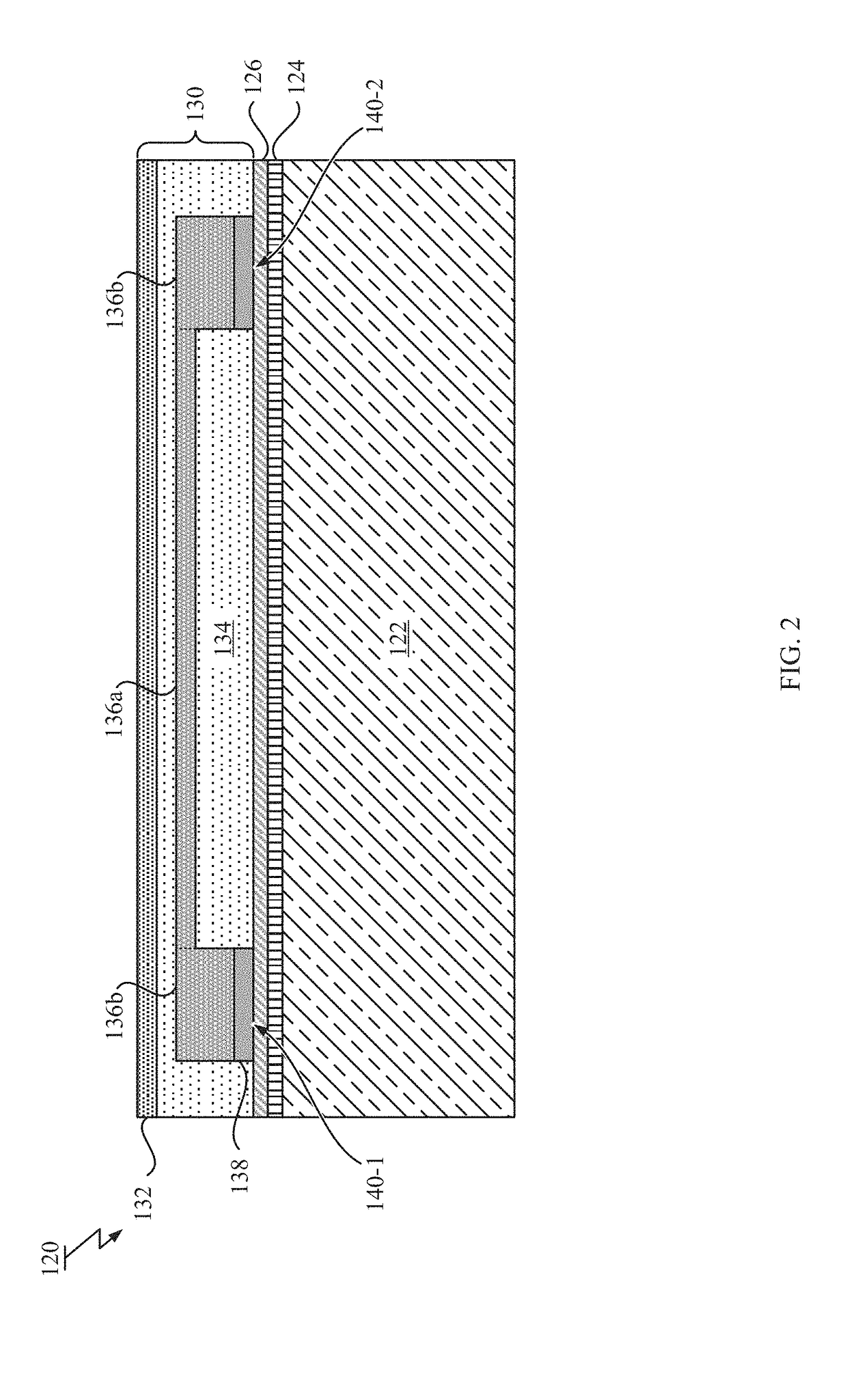
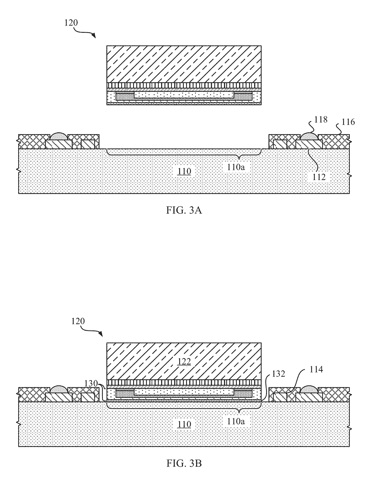
[0062]Hereinafter, referring to FIGS. 1A, 1B, a schematic of an interconnection substrate according to an exemplary embodiment of the present invention is described.

[0063]FIGS. 1A, 1B il...


PUM


Abstract

A technique for interconnecting chips by using an interconnection substrate is disclosed. The interconnection substrate includes a base substrate, a first group of electrodes on the base substrate for a first chip to be mounted, and a second group of electrodes on the base substrate for a second chip to be mounted. The interconnection substrate further includes an interconnection layer that includes a first set of pads for the first chip, a second set of pads for the second chip, traces and an organic insulating material. The interconnection layer is disposed on the base substrate and located within a defined area on the base substrate between the first group of electrodes and the second group of the electrodes.

Description

BACKGROUNDTechnical Field[0001]The present invention, generally, relates to interconnection technology, more particularly, to an interconnection substrate used for interconnecting chips mounted thereon, an electronic device including the interconnection substrate, an interconnection layer carrying structure and methods of fabricating thereof.Description of Related Art[0002]In response to growing demand for wide band signal transmission between chips (or dice), several technologies targeting high density interconnections between chips have been proposed, including silicon interposer, EMIB (Embedded Multi-Die Interconnect Bridge) and iTHOP (integrated Thin film High density Organic Package).[0003]The silicon interposer technology requires an expensive BEOL (Back End Of Line) process to form high density circuitries on the silicon interposer and a TSV (Through Silicon Via) fabrication process to connect metallization layers on its front and back surfaces. Also large insertion loss is c...

Claims


Application Information

Patent Timeline
IPC IPC(8): H01L23/538H01L23/00H01L25/065H01L25/00H01L21/48
CPCH01L23/5386H01L24/16H01L24/50H01L24/73H01L25/0655H01L2224/73211H01L23/5383H01L21/4857H01L21/4853H01L21/481H01L2224/16227H01L25/50H01L23/544H01L21/6835H01L2221/68359H01L2221/68381H01L2223/54426H01L2924/15311H01L2924/15192H01L2224/32225H01L2224/73204H01L2224/92125H01L2224/81191H01L2224/81193H01L2224/13082H01L2224/0401H01L2224/81815H01L2224/81203H01L24/13H01L24/32H01L24/81H01L24/92H01L23/5384H01L21/4846H01L2224/13147H01L2224/81444H01L2224/131H01L2224/13111H01L2224/2919H01L2224/16225H01L2924/00H01L2924/00014H01L2924/014H01L2924/069H01L2924/0665
Inventor HORIBE, AKIHIROMORI, HIROYUKIOKAMOTO, KEISHI
Owner IBM CORP
Why Eureka
Try Eureka