Device and method of manufacture of an interconnection structure for printed circuit boards

a technology of interconnection structure and printed circuit board, which is applied in the direction of printed circuit parts, printed circuit non-printed electric components association, printed element electric connection formation, etc., to achieve the effects of reducing environmental impact, reducing manufacturing times and costs, and increasing flexibility in circuit design and adjustmen

Inactive Publication Date: 2005-12-29
JOY STEPHEN C
View PDF8 Cites 30 Cited by
  • Summary
  • Abstract
  • Description
  • Claims
  • Application Information

AI Technical Summary

Benefits of technology

[0014] Advantages of the invention over previously known art include reduced manufacturing times and costs, reduced environmental impact, increased flexibility in circuit design and adjustment, and improved component inventory control.

Problems solved by technology

However, many components manufactured according to newer technology do not employ leads configured to pass through a circuit board, but rather employ surface mounting techniques, which do not require plated-through-holes, but are rather affixed to pads formed on a face of a PCB.

Method used


Image

  • Device and method of manufacture of an interconnection structure for printed circuit boards
  • Device and method of manufacture of an interconnection structure for printed circuit boards
  • Device and method of manufacture of an interconnection structure for printed circuit boards

Examples


Embodiment Construction

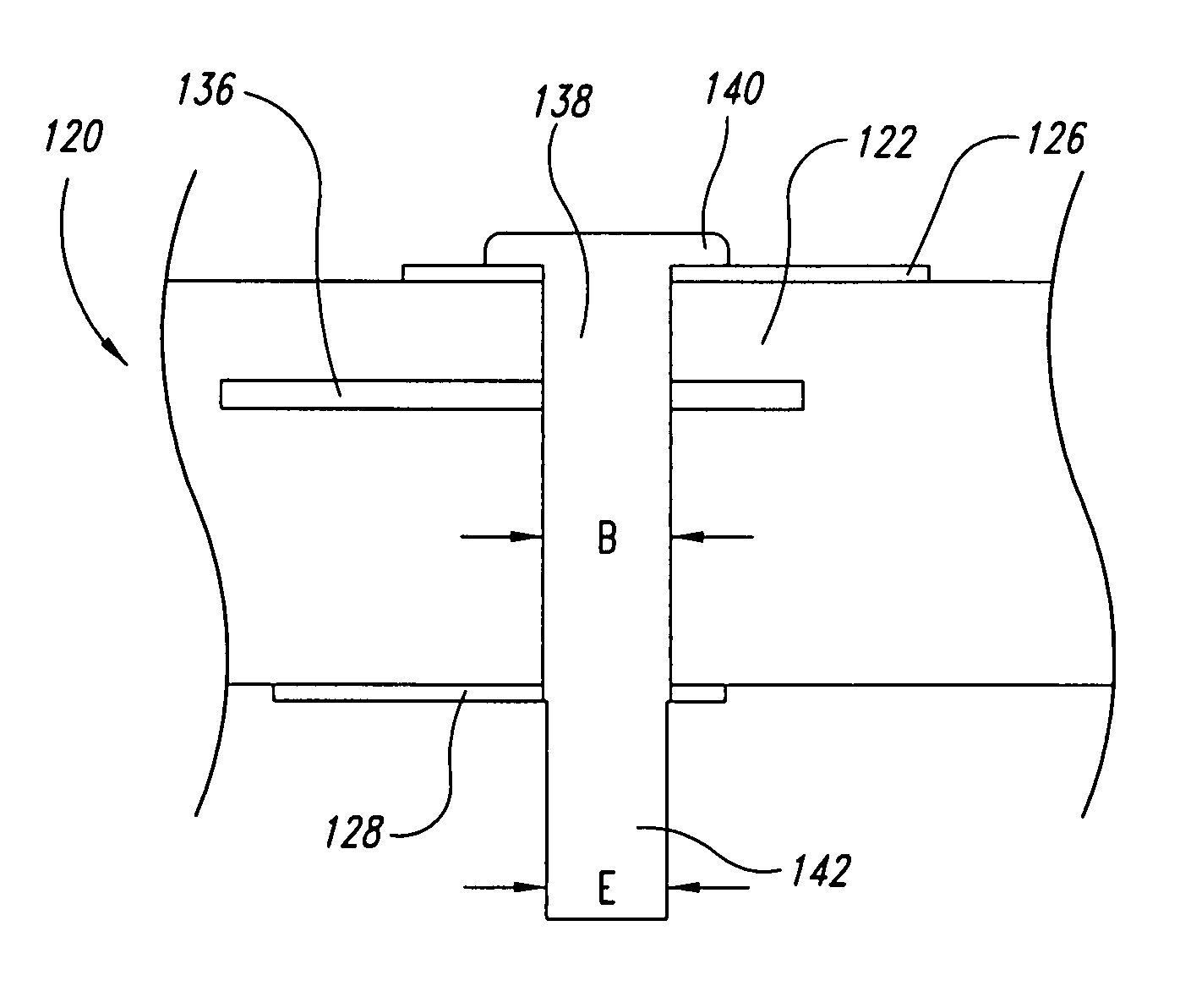
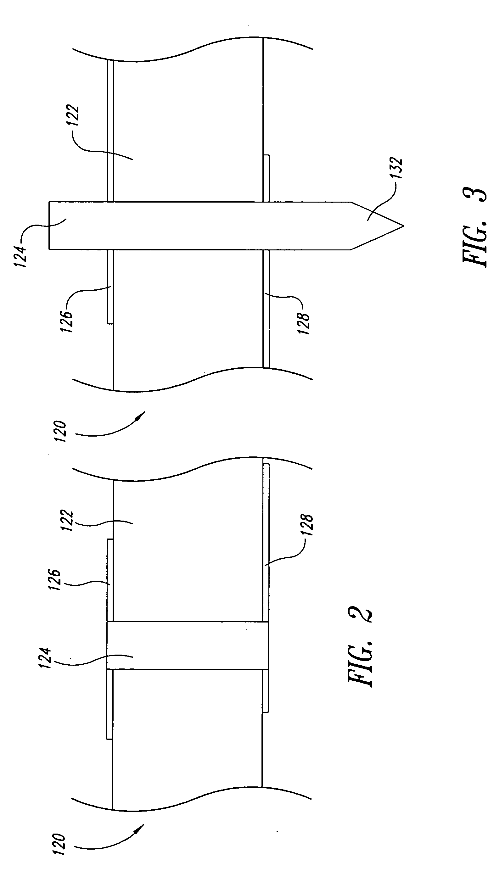
[0027] According to an embodiment of the invention, an interconnection structure is provided as illustrated in FIG. 2. A printed circuit board 120 having a substrate 122 is shown having upper and lower conductive layers 126, 128 and an interconnection pin 124 traversing the substrate 122 from one face to the other, and providing an electrically continuous connection between the upper and lower conductive layers 126, 128. According to one embodiment of the invention, the interconnection pin 124 is positioned in the substrate 122 and with the ends thereof flush with the surfaces 127, 129 of the PCB 120. Either or both of the surfaces 127, 129, may comprise outer surfaces of the upper and lower conductive layers 126, 128, respectively, or alternatively, may comprise outer surfaces of the non-conductive substrate 122.

[0028] While generally referred to simply as layers in this description, conductive layers 126, 128, as well as other conductive layers referred to herein, may comprise la...


PUM


Abstract

An interconnection structure for coupling conductive layers of a circuit board includes a pin configured to be press-fitted in an aperture traversing the circuit board, to electrically couple the conductive traces. The pin may be placed in a predrilled aperture, or driven into the circuit board, forming the aperture thereby. The pin may also be configured as a punch, removing a plug of material as it is driven therethrough. The pin may comprise a capacitive or resistive region configured to capacitively or resistively couple the first and second traces. The pin may be configured such that capacitive or resistive values are selectable according to a depth to which the pin is positioned in the aperture. The pin may serve as an offset post for mounting the circuit board to a chassis. In such a case, the pin may be provided with a longitudinal aperture configured to receive a threaded screw.

Description

BACKGROUND OF THE INVENTION [0001] 1. Field of the Invention [0002] This patent application is directed generally to the field of circuit board manufacture, and in particular to structures for interconnecting conductive layers thereof. [0003] 2. Description of the Related Art [0004] Most modern electronic systems employ one or more printed circuit boards (PCB's) of varying degrees of complexity. For example, some simple electronic devices employ circuit boards having a single conductive layer laminated to one of the faces thereof, from which a circuit is etched. Other devices employ circuit boards having conductive layers laminated on opposing faces thereof, each of which is etched with a different circuit pattern. More complex circuit boards, employing internal conductive layers, as well as conductive layers on each outer surface, are well known in the art. [0005] In circuit boards employing more than a single conductive layer, means for interconnecting the various conductive layer...

Claims


Application Information

Patent Timeline
Patent Type & Authority Applications(United States)
IPC IPC(8): H05K1/18H05K3/30H05K3/34H05K3/40
CPCH05K1/184H05K2203/1189H05K3/3447H05K3/4046H05K2201/092H05K2201/09645H05K2201/09809H05K2201/10015H05K2201/10022H05K2201/10242H05K2201/10303H05K2201/1059H05K2201/1081H05K2201/10893H05K2203/1115H05K3/308
Inventor JOY, STEPHEN C.
Owner JOY STEPHEN C
Why Eureka
Try Eureka