

Method for fabricating semiconductor packages
a technology for semiconductor packages and semiconductor components, applied in semiconductor devices, semiconductor/solid-state device details, electrical apparatus, etc., can solve the problems of significant difficulty in fabrication of bga semiconductor packages, waste of substrate utilization, and increased overall cost by about 15 to 20%, and achieves easy separation, poor adhesion, and convenient fabrication
- Summary
- Abstract
- Description
- Claims
- Application Information
AI Technical Summary
Benefits of technology
Problems solved by technology
Method used
Image

Examples
first preferred embodiment
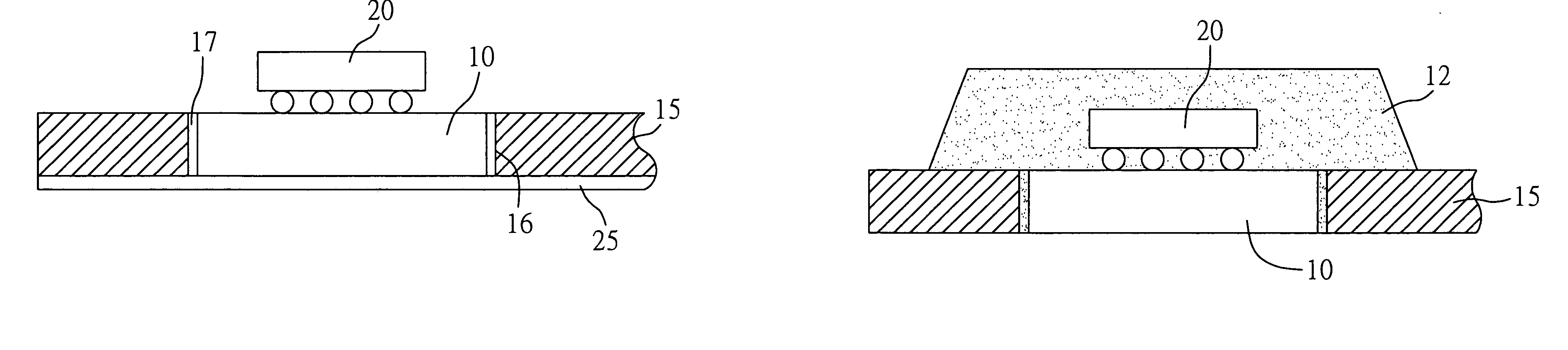
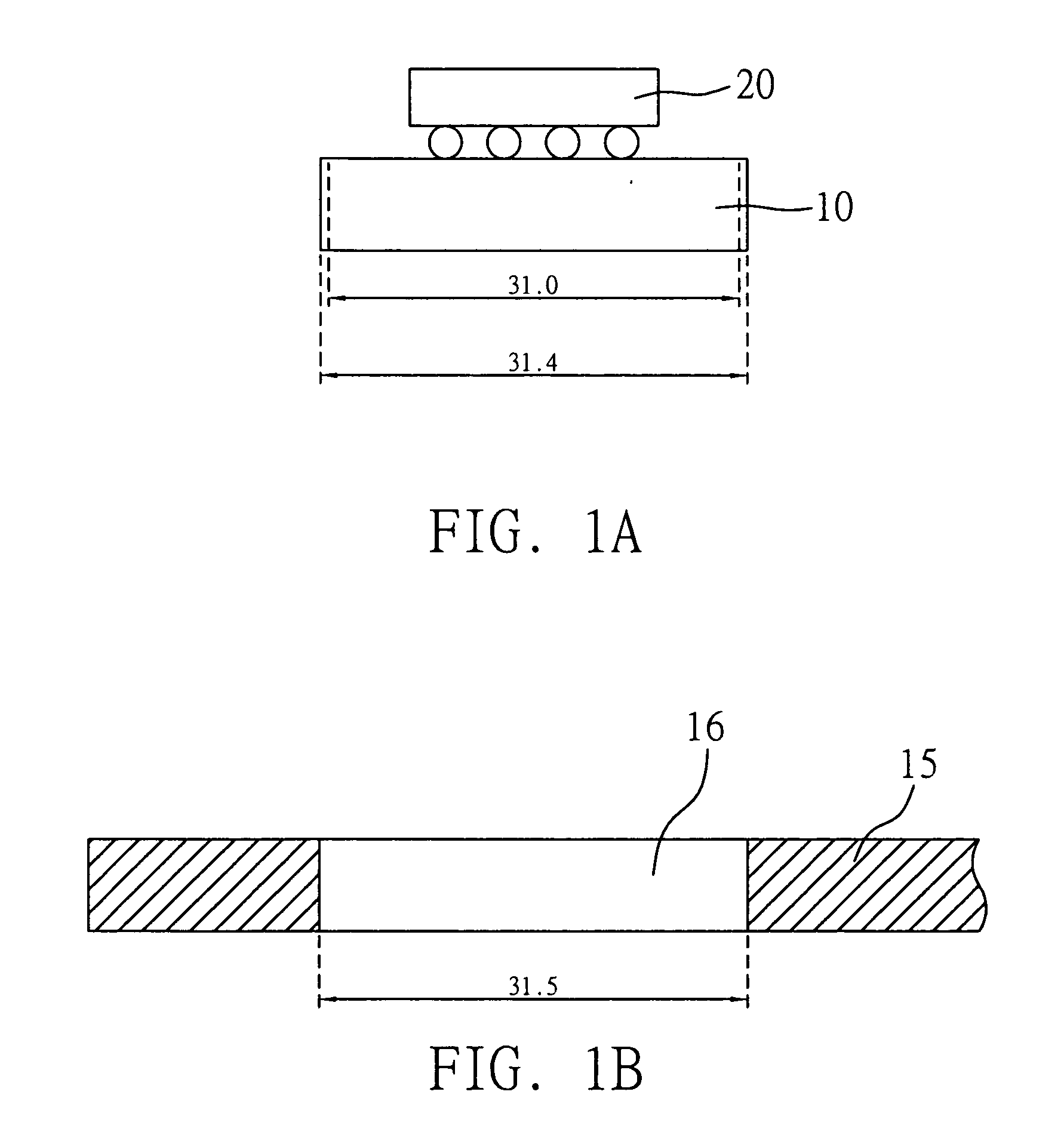
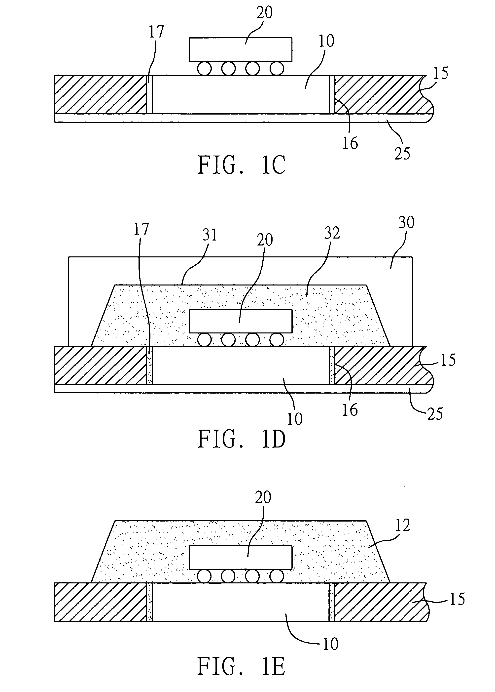
[0029]FIGS. 1A to 1H show steps of a method for fabricating semiconductor packages according to a first preferred embodiment of the present invention. Referring to FIG. 1A, firstly, a plurality of build-up substrates 10 (only one is shown) each carrying at least one chip 20 thereon are prepared. Each of the substrates 10 has slightly larger length and width than the predetermined length and width of a final semiconductor package 1 (shown in FIG. 1H) respectively. In this embodiment, the predetermined dimensions of the semiconductor package 1 after singulation are 31 mm×31 mm in length and width, such that the length and width of the substrate 10 are sized 31.4 mm×31.4 mm. Then, referring to FIG. 1B, a substrate carrier 15 having a plurality of openings 16 (only one is shown) is prepared, wherein each of the openings 16 is larger in length and width than each of the substrates 10, such that the substrates 10 carrying the chips 20 thereon can be embedded and positioned in the correspo...
second preferred embodiment
[0035] Apart from the above first embodiment in which the substrate 10 has slightly larger length and width than the predetermined length and width of the semiconductor package 1, the substrate 10 can be sized slightly smaller in length and width than the semiconductor package 1 to further reduce the material used for the substrate 10 according to a second preferred embodiment shown in FIGS. 4A to 4H wherein similarly, the predetermined size of the semiconductor package 1 after singulation is 31 mm×31 mm in length and width.
[0036] Referring to FIG. 4A, firstly, a plurality of build-up substrates 10 (only one is shown) each carrying at least one chip 20 thereon are prepared. Each of the substrates 10 has its length and width sized 30.8 mm×30.8 mm and slightly smaller than the predetermined length and width of the semiconductor package 1 (31 mm×31 mm as shown in FIG. 4H). Referring to FIG. 4B, a carrier 15 having a plurality of openings 16 (only one is shown) is prepared. Each of the...
third preferred embodiment
[0040] Apart from the carrier 15 made of an organic insulating material such as FR4, FR5, BT, and so on, a metal carrier having a metal layer plated on a surface thereof can be used in the present invention according to a third preferred embodiment shown in FIGS. 5A to 5I. The metal layer is made of a material poorly adhesive to the encapsulant 32. In the third embodiment, the predetermined size of the semiconductor package 1, the size of the substrate 10, and the size of an opening 46 of a carrier 45 are all same as those described in the foregoing embodiments. Only the material used for the carrier 45 and some of the fabrication processes in the third embodiment are different from those in the foregoing embodiments.
[0041] Referring to FIG. 5A, firstly, a plurality of build-up substrates 10 (only one is shown) each carrying at least one chip 20 thereon are prepared. The length and width of each of the substrates 10 are 31.4 mm×31.4 mm, and the predetermined length and width of the...
PUM
 Abstract
Description
Claims
Application Information